封装信息
| CAD 模型: | View CAD Model |
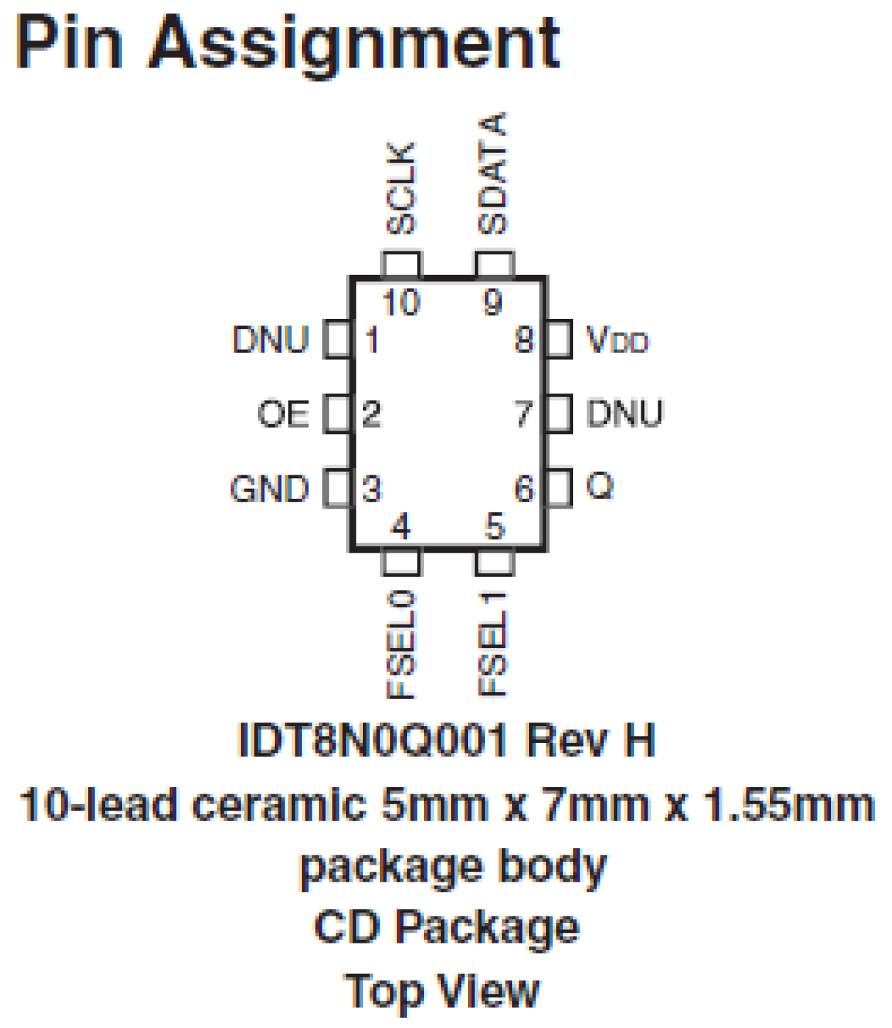
| Pkg. Type: | CLCC |
| Pkg. Code: | CD10 |
| Lead Count (#): | 10 |
| Pkg. Dimensions (mm): | 7.0 x 5.0 x 1.5 |
| Pitch (mm): | 2.54 |
环境和出口类别
| Moisture Sensitivity Level (MSL) | 1 |
| Pb (Lead) Free | Yes |
| ECCN (US) | EAR99 |
| HTS (US) | 8542.39.0090 |
产品属性
| Lead Count (#) | 10 |
| Carrier Type | Tray |
| Moisture Sensitivity Level (MSL) | 1 |
| Pb (Lead) Free | Yes |
| Pb Free Category | e4 Au |
| Temp. Range (°C) | -40 to 85°C |
| Advanced Features | Programmable Clock |
| C-C Jitter Max P-P (ps) | 20 |
| C-C Jitter Typ P-P (ps) | 7 |
| Core Voltage (V) | 3.3 |
| Family Name | FemtoClock NG |
| Freq. Accuracy Init. (± PPM) | 50 |
| Freq. Accuracy Temp. (± PPM) | 20 |
| Freq. Stability Total (± PPM) | 33 |
| Function | XO |
| Length (mm) | 7 |
| MOQ | 364 |
| Output Banks (#) | 1 |
| Output Freq Range (MHz) | 15.476 - 260 |
| Output Signaling | LVCMOS |
| Output Type | LVCMOS |
| Output Voltage (V) | 3.3 |
| Outputs (#) | 1 |
| Package Area (mm²) | 35 |
| Period Jitter Max P-P (ps) | 4 |
| Period Jitter Typ P-P (ps) | 2 |
| Phase Jitter Max RMS (fs) | 285 |
| Phase Jitter Max RMS (ps) | 0.285 |
| Phase Jitter Typ RMS (fs) | 250 |
| Phase Jitter Typ RMS (ps) | 0.25 |
| Pitch (mm) | 2.54 |
| Pkg. Dimensions (mm) | 7.0 x 5.0 x 1.5 |
| Pkg. Type | CLCC |
| Product Category | Crystal Oscillators |
| Prog. Clock | Yes |
| Prog. Interface | I2C |
| Qty. per Carrier (#) | 364 |
| Qty. per Reel (#) | 0 |
| Requires Terms and Conditions | Does not require acceptance of Terms and Conditions |
| Supply Voltage (V) | 2.5 - 2.5, 3.3 - 3.3 |
| Tape & Reel | No |
| Thickness (mm) | 1.5 |
| VCO Max Freq (MHz) | 2600 |
| VCO Min Freq (MHz) | 1950 |
| Width (mm) | 5 |
有关 8N0Q001 的资源
描述
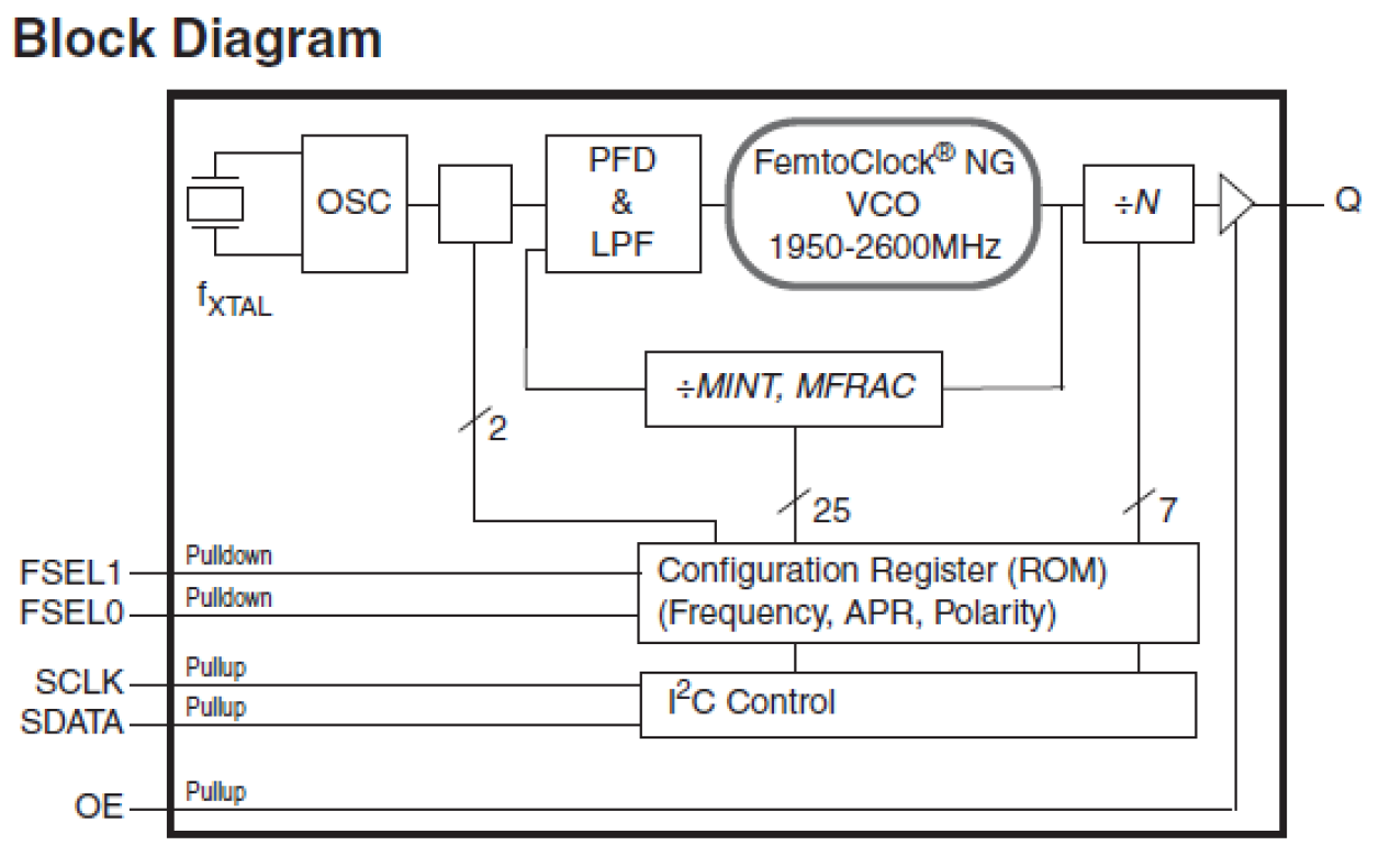
The 8N0Q001 is a quad-frequency programmable clock oscillator with very flexible frequency programming capabilities. The device uses Renesas' fourth-generation FemtoClock®NG technology for an optimum of high clock frequency and low phase noise performance. The device accepts 2.5V or 3.3V supply and is packaged in a small, lead-free (RoHS 6) 10-lead ceramic 5mm x 7mm x 1.55mm package.
Besides the four default power-up frequencies set by the FSEL0 and FSEL1 pins, the 8N0Q001 can be programmed via the I2C interface to output clock frequencies between 15.476MHz and 260MHz to a very high degree of precision with a frequency step size of 435.9Hz ÷ N (N: PLL post divider). Since the FSEL0 and FSEL1 pins are mapped to four independent PLL M and N divider registers (P, MINT, MFRAC, and N), reprogramming those registers to other frequencies under control of FSEL0 and FSEL1 is supported. The extended temperature range supports wireless infrastructure, telecommunication, and networking end equipment requirements.


