特性
- 0.3ps RMS typical jitter (including spurs), 12kHz to 20MHz
- Operating modes: locked to input signal and free-run
- Digitally Controlled Oscillator (DCO) mode for software adjustment of operating frequency
- Operates from a 10MHz to 40MHz fundamental-mode crystal
- Accepts one LVPECL, LVDS, LVHSTL, HCSL, or LVCMOS input clock
- Accepts frequencies ranging from 10MHz up to 600MHz
- Clock input monitoring
- Generates 12 LVPEC/LVDS/HCSL or 24 LVCMOS output clocks
- Output frequencies ranging from 8kHz up to 1.0GHz (diff)
- Output frequencies ranging from 8kHz up to 250MHz (LVCMOS)
- Two Output Enable control inputs
- Lock and Loss-of-Signal status outputs
- Programmable output de-skew adjustments in steps as small as 16ps
- Register programmable through I²C or via external I²C EEPROM
- Bypass clock paths and reference output for system tests
- -40 °C to +85 °C ambient operating temperature
- Packaged in a 72-pin QFN, lead-free RoHS (6)
- Supported by Renesas' Timing Commander Software


描述
The 8T49N1012 has one fractional-feedback PLL that can be used for frequency synthesis. It is equipped with two integer and eight fractional output dividers, allowing the generation of up to ten different output frequencies, ranging from 8kHz to 1GHz. Eight of these frequencies are completely independent of each other and the inputs. Two more are related frequencies. The twelve outputs may select among LVPECL, LVDS, HSCL, or LVCMOS output levels.
This functionality makes it ideal to be used in any frequency synthesis application, including 1G, 10G, 40G, and 100G Synchronous Ethernet, OTN, and SONET/SDH, including ITU-T G.709 (2009) FEC rates. The device supports Output Enable inputs and Lock and LOS status outputs.
应用
- OTN or SONET/SDH equipment line cards (up to OC-192, and supporting FEC ratios)
- Gigabit and Terabit IP switches/routers
- Wireless base station baseband
- Data communications
Renesas Boards & Kits
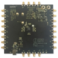
Evaluation Kit for 8T49N1012
The EVK-8T49N1012 evaluation board kit is a platform that is designed to help the customer evaluate Renesas's 8T49N1012 FemtoClockR NG 12-output Frequency Synthesizer. When the board is connected to a PC running Renesas' Timing CommanderTM software through USB, the device can be configured and... 阅读详情
