封装信息
| CAD 模型: | View CAD Model |
| Pkg. Type: | VFQFPN |
| Pkg. Code: | NLG56 |
| Lead Count (#): | 56 |
| Pkg. Dimensions (mm): | 8.0 x 8.0 x 0.85 |
| Pitch (mm): | 0.5 |
环境和出口类别
| Moisture Sensitivity Level (MSL) | 3 |
| Pb (Lead) Free | Yes |
| ECCN (US) | EAR99 |
| HTS (US) | 8542.39.0090 |
产品属性
| Lead Count (#) | 56 |
| Carrier Type | Reel |
| Moisture Sensitivity Level (MSL) | 3 |
| Qty. per Reel (#) | 3000 |
| Qty. per Carrier (#) | 0 |
| Pb (Lead) Free | Yes |
| Pb Free Category | e3 Sn |
| Temp. Range (°C) | -40 to 85°C |
| Advanced Features | Programmable Clock |
| Core Voltage (V) | 3.3 |
| Divider Value | 2 |
| Family Name | FemtoClock NG |
| Feedback Divider | 16 - 250 |
| Input Freq (MHz) | 25 - 100 |
| Input Type | Crystal, LVPECL, LVDS, LVCMOS |
| Inputs (#) | 2 |
| Length (mm) | 8 |
| MOQ | 3000 |
| Output Banks (#) | 1 |
| Output Freq Range (MHz) | 156.25 - 1250 |
| Output Signaling | LVPECL, LVDS |
| Output Skew (ps) | 20 |
| Output Type | LVPECL, LVDS |
| Output Voltage (V) | 3.3 |
| Outputs (#) | 10 |
| Package Area (mm²) | 64 |
| Phase Jitter Max RMS (fs) | 128 |
| Phase Jitter Max RMS (ps) | 0.128 |
| Phase Jitter Typ RMS (fs) | 84 |
| Phase Jitter Typ RMS (ps) | 0.084 |
| Pitch (mm) | 0.5 |
| Pkg. Dimensions (mm) | 8.0 x 8.0 x 0.85 |
| Pkg. Type | VFQFPN |
| Prog. Clock | Yes |
| Prog. Interface | I2C |
| Reel Size (in) | 13 |
| Reference Output | No |
| Requires Terms and Conditions | Does not require acceptance of Terms and Conditions |
| Spread Spectrum | No |
| Tape & Reel | Yes |
| Thickness (mm) | 0.85 |
| VCO Max Freq (MHz) | 2500 |
| VCO Min Freq (MHz) | 1910 |
| Width (mm) | 8 |
| Xtal Freq (KHz) | 10 - 40 |
| Xtal Inputs (#) | 1 |
| 已发布 | No |
有关 8T49NS010 的资源
描述
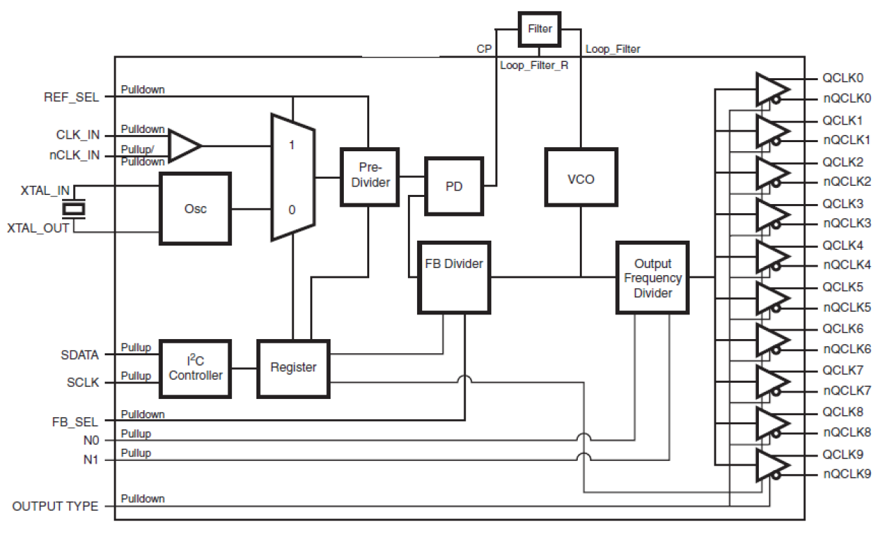
The 8T49NS010 is a clock synthesizer and fanout buffer/divider. When used with an external crystal, the 8T49NS010 generates high-performance timing geared towards the communications and datacom markets, especially for applications demanding extremely low phase noise jitter, such as 10, 40, and 100GE.
The 8T49NS010 provides versatile frequency configurations and output formats and is optimized to deliver excellent phase noise performance. The device delivers an optimum combination of high clock frequency and low phase noise performance, combined with high power supply noise rejection.


