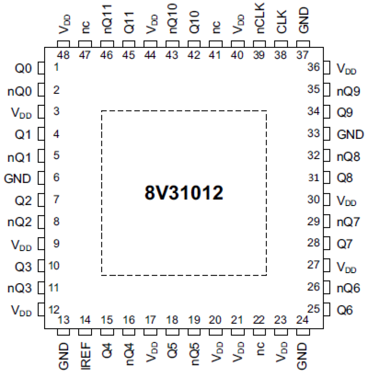
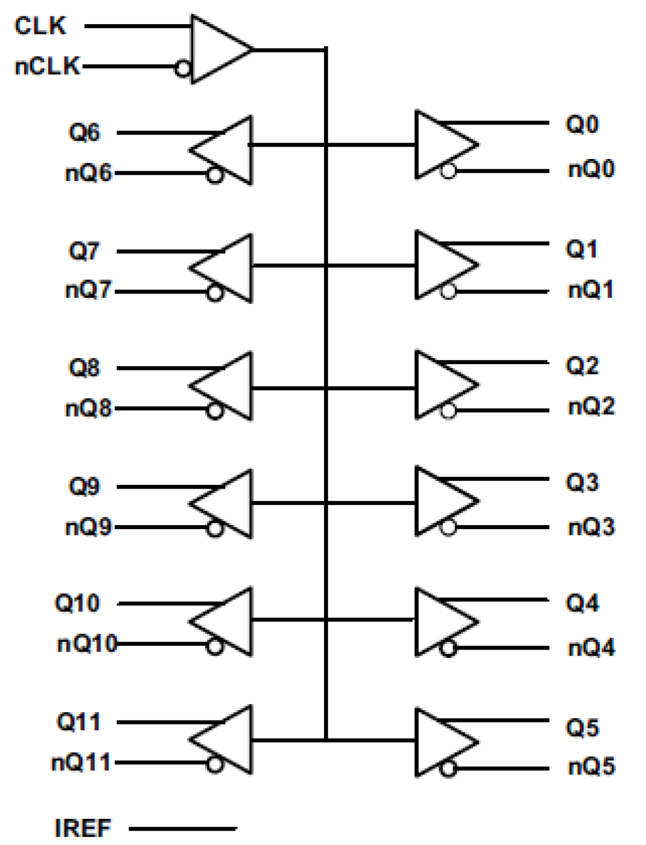
特性
- Twelve differential HCSL outputs
- Translates any differential input signal (LVPECL, LVHSTL, LVDS, HCSL) to HCSL levels without external bias networks
- Maximum output frequency: 250MHz
- Output skew: 265ps (typical)
- VOH: 850mV (maximum)
- Full 3.3V supply voltage
- Available in a lead-free (RoHS 6) package
- -40 °C to 85 °C ambient operating temperature
描述
The 8V31012 is a 1-to-12 differential HCSL fanout buffer designed to translate any differential signal levels to differential HCSL output levels. An external reference resistor is used to set the value of the current supplied to an external load/termination resistor. The load resistor value is chosen to equal the value of the characteristic line impedance of 50Ω. The 8V31012 is characterized to an operating supply voltage of 3.3V.
The differential HCSL outputs, accurate crossover voltage, and duty cycle make the 8V31012 ideal for interfacing to PCI Express and FBDIMM applications.
当前筛选条件
筛选
软件与工具
样例程序
模拟模型
This is the first video in our PCIe series. In this video, we define PCIe architectures, focusing on common and separate clock architectures. Watch the rest of the video series below where Ron will cover the impact of different timing architectures.
In this episode, Ron Wade from IDT (acquired by Renesas) explains PCIe common clocking and its impact on timing solutions. Learn about using a single clock source, fan-out buffers, and the considerations for spread spectrum and non-spread spectrum clocking in PCIe systems.
In this video, we explore PCIe with separate reference clocks and the effects of clock selection. Learn how separate reference clocks work and their impact on system performance and stability.
This video provides a high-level overview of Separate Reference Clock with Independent Spread (SRIS) architectures for PCI Express systems, additional performance requirements that this clocking architecture imposes on the reference clocks, and some system implications encountered trying to implement the architecture.
A brief overview of how data rates have changed from PCI Express (PCIe) Generation 1, Gen 2, Gen 3, Gen 4 and Gen 5.
Presented by Ron Wade, system architect at IDT. For more information about IDT's PCIe timing solutions, visit the PCI Express (PCIe) Clocks page.
A brief overview of how clock and timing specifications have changed from PCI Express (PCIe) Generation 1, Gen 2, Gen 3, Gen 4 and Gen 5.
Presented by Ron Wade, system architect at IDT (acquired by Renesas). For more information, visit Renesas's PCIe Timing Solutions page.
A brief overview of the PCI Express common clock (CC) jitter model, and the transfer functions as they relate to the timing PLLs. This model applies to PCI Express (PCIe) Gen 2, Gen 3, Gen 4 and Gen 5. The equations would be slightly different for other PCIe architectures, such as SRIS, SRnS, or data clocked.
Presented by Ron Wade, system architect at IDT (acquired by Renesas). For more information about Renesas's PCIe timing solutions, visit the PCI Express (PCIe) Clocks page.