封装信息
| CAD 模型: | View CAD Model |
| Pkg. Type: | VFQFPN |
| Pkg. Code: | NLG48 |
| Lead Count (#): | 48 |
| Pkg. Dimensions (mm): | 7.0 x 7.0 x 0.9 |
| Pitch (mm): | 0.5 |
环境和出口类别
| Moisture Sensitivity Level (MSL) | 3 |
| Pb (Lead) Free | Yes |
| ECCN (US) | EAR99 |
| HTS (US) | 8542.39.0090 |
产品属性
| Lead Count (#) | 48 |
| Carrier Type | Tray |
| Moisture Sensitivity Level (MSL) | 3 |
| Qty. per Reel (#) | 0 |
| Qty. per Carrier (#) | 260 |
| Pb (Lead) Free | Yes |
| Pb Free Category | e3 Sn |
| Temp. Range (°C) | -40 to 85°C |
| 100M Non-SSC Outputs | 2 |
| 25M Outputs | 3 |
| C-C Jitter Max P-P (ps) | 16 |
| C-C Jitter Typ P-P (ps) | 9 |
| Core Voltage (V) | 3.3 |
| Feedback Input | No |
| Function | Clock Generator |
| Input Freq (MHz) | 25 - 25 |
| Input Type | LVCMOS, Crystal |
| Inputs (#) | 2 |
| Length (mm) | 7 |
| MOQ | 260 |
| Output Banks (#) | 4 |
| Output Freq Range (MHz) | 15 - 15, 50 - 50, 100 - 100, 125 - 125 |
| Output Signaling | LVDS, LVCMOS |
| Output Skew (ps) | 30 |
| Output Type | LVDS, LVCMOS |
| Output Voltage (V) | 3.3V, 2.5V, 1.8V |
| Outputs (#) | 10 |
| Package Area (mm²) | 49 |
| Period Jitter Max P-P (ps) | 8.1 |
| Period Jitter Typ P-P (ps) | 3 |
| Phase Jitter Max RMS (ps) | 0.8 |
| Phase Jitter Typ RMS (ps) | 0.57 |
| Pitch (mm) | 0.5 |
| Pkg. Dimensions (mm) | 7.0 x 7.0 x 0.9 |
| Pkg. Type | VFQFPN |
| Product Category | Low Jitter Clocks (<700 fs RMS), General Purpose Clocks |
| Prog. Clock | No |
| Prog. Interface | NO |
| Reference Output | Yes |
| Requires Terms and Conditions | Does not require acceptance of Terms and Conditions |
| Spread Spectrum | No |
| Supply Voltage (V) | 3.3 - 3.3 |
| Tape & Reel | No |
| Thickness (mm) | 0.9 |
| Width (mm) | 7 |
| Xtal Freq (KHz) | 25000 - 25000 |
| Xtal Freq (MHz) | 25 - 25 |
| Xtal Inputs (#) | 1 |
有关 8V44S269 的资源
描述
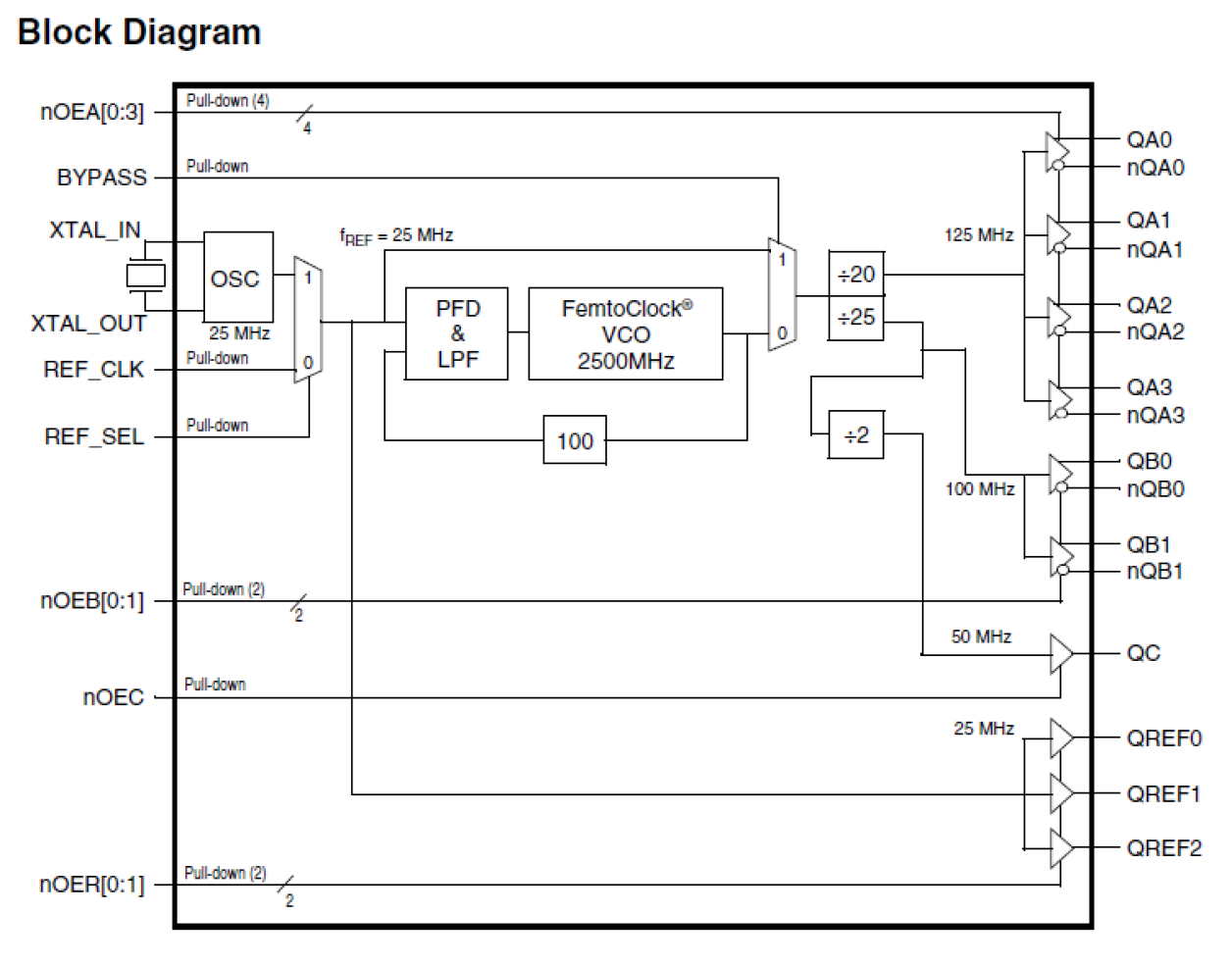
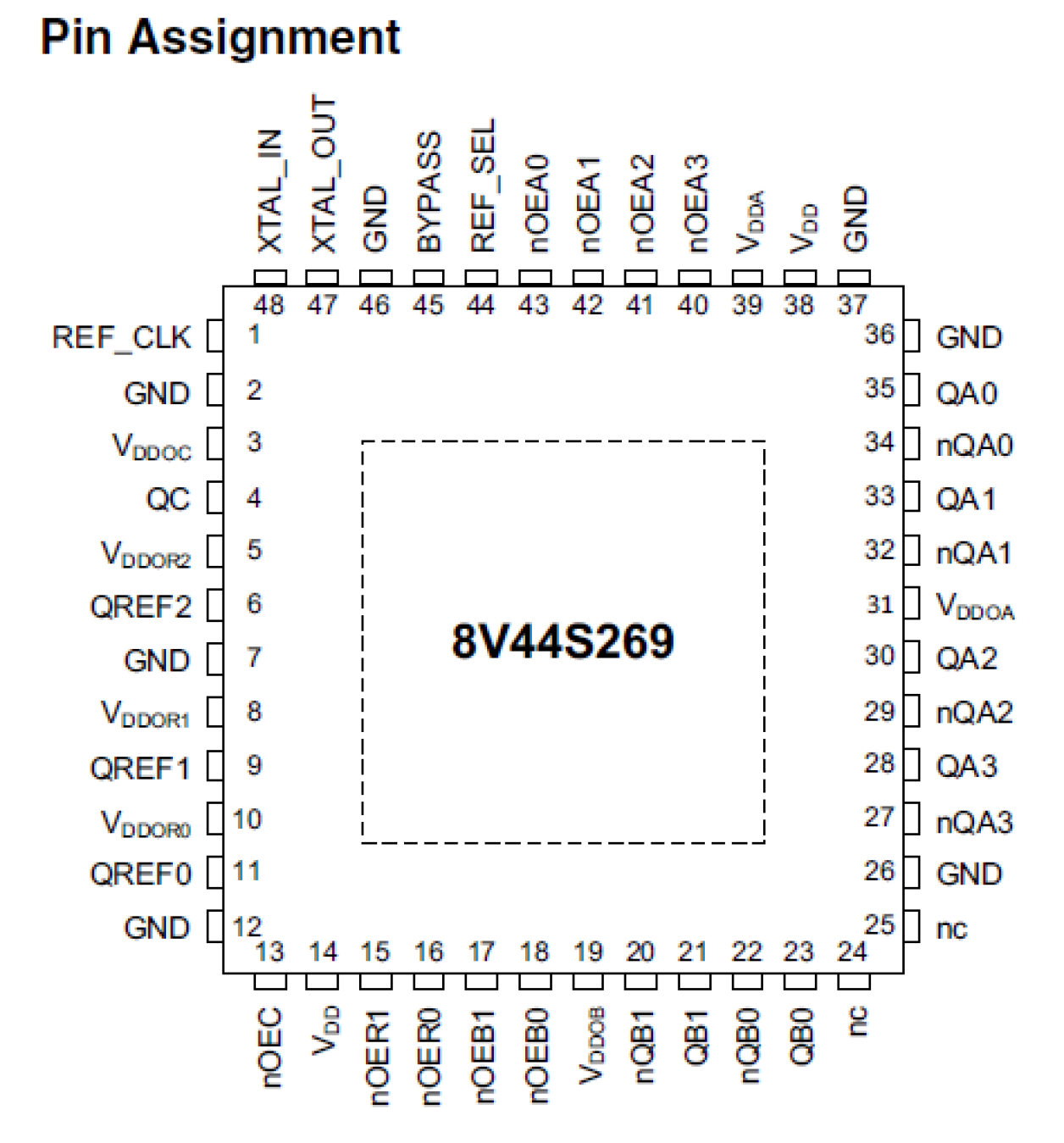
The 8V44S269 is a ten LVDS/LVTTL output clock synthesizer designed for instrumentation and wireless applications. The device generates four copies of a 125MHz, two copies of a 100MHz differential LVDS clock, and one 50MHz (LVCMOS) signal with excellent phase jitter performance. The PLL is optimized for a reference frequency of 25MHz. Both a crystal interface and a single-ended input are supported for the reference frequency. Three LVCMOS outputs duplicate the reference frequency and are provided for clock tree cascade purposes. Each of the four LVCMOS outputs can be supplied with either 3.3V, 2.5V, or 1.8V, forming the respective LVCMOS output levels of 3.3V, 2.5V, or 1.8V. The device uses Renesas' third-generation FemtoClock® technology for an optimum of high clock frequency and low phase noise performance, combined with a low power consumption. The device supports a 3.3V voltage supply and is packaged in a small, lead-free (RoHS 6) 48-lead VFQFN package.

