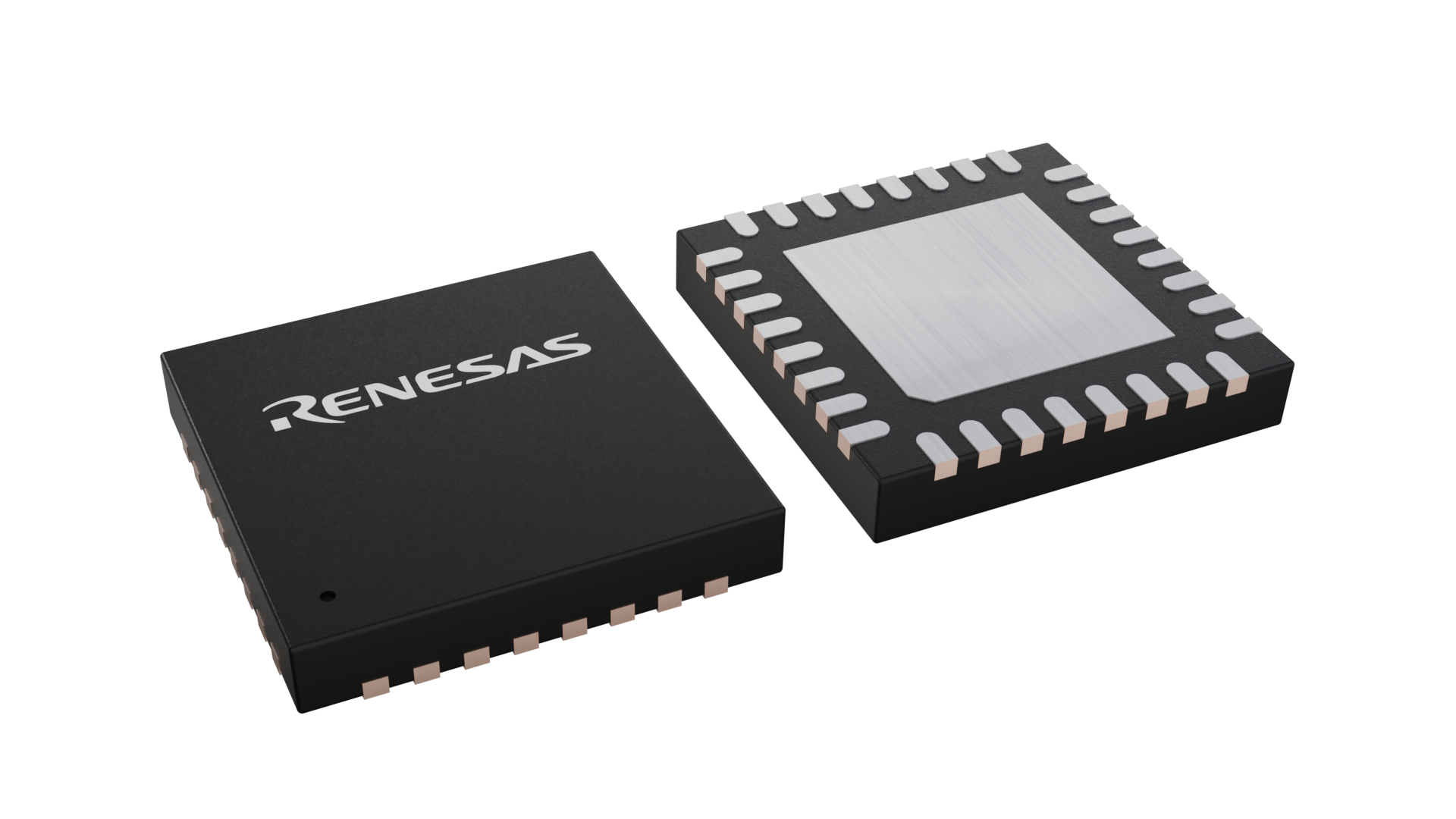
封装信息
| CAD 模型: | View CAD Model |
| Pkg. Type: | VFQFPN |
| Pkg. Code: | NLG32 |
| Lead Count (#): | 32 |
| Pkg. Dimensions (mm): | 5.0 x 5.0 x 0.9 |
| Pitch (mm): | 0.5 |
环境和出口类别
| Moisture Sensitivity Level (MSL) | 3 |
| Pb (Lead) Free | Yes |
| ECCN (US) | EAR99 |
| HTS (US) | 8542.39.0090 |
产品属性
| Lead Count (#) | 32 |
| Carrier Type | Reel |
| Moisture Sensitivity Level (MSL) | 3 |
| Advanced Features | Selectable Output Impedance, Very Low Additive Jitter, Selectable Output Amplitude |
| Qty. per Reel (#) | 2500 |
| Qty. per Carrier (#) | 0 |
| Pb (Lead) Free | Yes |
| Pb Free Category | e3 Sn |
| Temp. Range (°C) | -40 to 85°C |
| Country of Assembly | MALAYSIA |
| Country of Wafer Fabrication | SINGAPORE |
| Accepts Spread Spec Input | Yes |
| Additive Phase Jitter Typ RMS (fs) | 78 |
| Additive Phase Jitter Typ RMS (ps) | 0.078 |
| App Jitter Compliance | PCIe Gen1, PCIe Gen2, PCIe Gen3, PCIe Gen4, PCIe Gen5, PCIe Gen6 |
| Architecture | Common, SRNS, SRIS |
| Core Voltage (V) | 3.3V, 2.5V, 1.8V |
| Diff. Input Signaling | HCSL, LVPECL, LVDS, LVCMOS |
| Diff. Inputs | 4 |
| Diff. Output Signaling | LP-HCSL |
| Diff. Outputs | 4 |
| Diff. Termination Resistors | 0 |
| Feedback Input | No |
| Function | Multiplexer |
| Input Freq (MHz) | 1.0E-6 - 350 |
| Input Type | HCSL |
| Inputs (#) | 4 |
| Length (mm) | 5 |
| Longevity | 2040 4月 |
| MOQ | 2500 |
| Output Banks (#) | 2 |
| Output Freq Range (MHz) | 1 - 200 |
| Output Impedance | 85, 100 |
| Output Skew (ps) | 22 |
| Output Type | LP-HCSL |
| Output Voltage (V) | 3.3V, 2.5V, 1.8V |
| Outputs (#) | 4 |
| PLL | No |
| Package Area (mm²) | 16 |
| Pitch (mm) | 0.5 |
| Pkg. Dimensions (mm) | 5.0 x 5.0 x 0.9 |
| Pkg. Type | VFQFPN |
| Power Consumption Typ (mW) | 124 |
| Price (USD) | $4.30978 |
| Prog. Clock | No |
| Reel Size (in) | 13 |
| Reference Output | No |
| Spread Spectrum | Yes |
| Supply Voltage (V) | 3.3 - 3.3, 2.5 - 2.5, 1.8 - 1.8 |
| Tape & Reel | Yes |
| Thickness (mm) | 0.9 |
| Width (mm) | 5 |
| 已发布 | No |
有关 9DML4493 的资源
描述
The 9DML4493A is a Gen1–7 compliant 4-input, 4-output clock multiplexer. It can also operate as a dual 2-input, 2-output clock multiplexer. It has very low additive phase jitter and is suitable for all PCIe data rates. The device supports today's complex system power sequencing requirements with Power Down Tolerant (PDT) and Flexible Power Sequencing (FPS) features.
For information regarding evaluation boards and material, please contact your local Renesas sales representative.
