特性
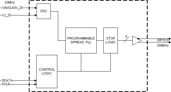
- 6 - 100 MHz Differential low power push pull (HCSL compatible) output pairs
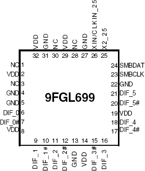
- 32-pin QFN; space-savings
- Push Pull outputs
- Low power consumption, reduced component count
- PCIe Gen2
- Spread spectrum capability; reduced EMI when needed
- D2/D3 SMBus Write/Read SMBus address
- Cycle-to-cycle jitter <125 ps
- Output-to-output skew < 100 ps
- Current consumption < 40 mA
- PCIe Gen2 phase jitter < 3.0 ps RMS
描述
The 9FGL699 is a 6-output low-power clock sythesizer for PCIe Gen2. It runs from a 25 MHz XTAL, provides spread spectrum capability, and has an SMBus for software control of the device.
当前筛选条件
筛选
软件与工具
样例程序
模拟模型
This is the first video in our PCIe series. In this video, we define PCIe architectures, focusing on common and separate clock architectures. Watch the rest of the video series below where Ron will cover the impact of different timing architectures.
In this episode, Ron Wade from IDT (acquired by Renesas) explains PCIe common clocking and its impact on timing solutions. Learn about using a single clock source, fan-out buffers, and the considerations for spread spectrum and non-spread spectrum clocking in PCIe systems.
In this video, we explore PCIe with separate reference clocks and the effects of clock selection. Learn how separate reference clocks work and their impact on system performance and stability.
This video provides a high-level overview of Separate Reference Clock with Independent Spread (SRIS) architectures for PCI Express systems, additional performance requirements that this clocking architecture imposes on the reference clocks, and some system implications encountered trying to implement the architecture.


