封装信息
| CAD 模型: | View CAD Model |
| Pkg. Type: | SOICN |
| Pkg. Code: | MTC |
| Lead Count (#): | 8 |
| Pkg. Dimensions (mm): | 4.9 x 3.9 x 0.00 |
| Pitch (mm): | 1.3 |
环境和出口类别
| Moisture Sensitivity Level (MSL) | 3 |
| Pb (Lead) Free | Yes |
| ECCN (US) | EAR99 |
| HTS (US) | 8542.33.0001 |
产品属性
| Pkg. Type | SOICN |
| Lead Count (#) | 8 |
| Carrier Type | Reel |
| Moisture Sensitivity Level (MSL) | 3 |
| Pb (Lead) Free | Yes |
| Pb Free Category | Pb-Free 100% Matte Tin Plate w/Anneal-e3 |
| MOQ | 2500 |
| Temp. Range (°C) | -55 to +125°C |
| CAGE code | 34371 |
| Country of Assembly | PHILIPPINES, MALAYSIA |
| Country of Wafer Fabrication | USA |
| AVOL (dB) | 100 |
| Bandwidth (MHz) | 0.5 |
| CMRR (dB) | 83 |
| Channels (#) | 1 |
| Die Sale Availability? | No |
| Enable | Strobe |
| Flow | Harsh Environment & MIL-STD-883 |
| Gain Min | 1 |
| IBIAS (nA) | 0.002 |
| IOUT (mA) | 2.7 |
| IS per Amp (mA) | 0.45 |
| Length (mm) | 4.9 |
| Noise VN (nV/√Hz) | 38 |
| Offset Voltage (Max) (mV) | 2 |
| Offset Voltage (max) | 2mV |
| PROTO Availability? | No |
| PSRR (db) | 83 |
| Pitch (mm) | 1.3 |
| Pkg. Dimensions (mm) | 4.9 x 3.9 x 0.00 |
| Qualification Level | Standard |
| Rail-to-Rail Input | Yes |
| Rail-to-Rail Input/Output | No |
| Rail-to-Rail Output | No |
| Rating | Harsh Environment |
| Single Supply Voltage Range (V) | 2 - 20 |
| Slew Rate (V/µs) | 0.5 |
| Supply Voltage (max) (V) | 20 - 20 |
| Supply Voltage (min) (V) | 2 - 2 |
| Thermal Shutdown | No |
| VOUT (V) | 19.75 |
| VS (Max) (V) | 20 |
| VS (Min) (V) | 2 |
| Width (mm) | 3.9 |
| field__slew_rate_typical_ | 0.5 |
有关 CA5420A 的资源
描述
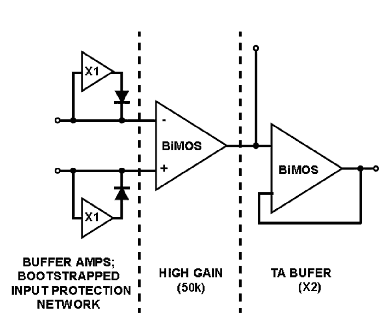
The CA5420A is an integrated circuit operational amplifier that combines PMOS transistors and bipolar transistors on a single monolithic chip. It is designed and guaranteed to operate in microprocessor logic systems that use V+ = 5V, V- = GND, since it can operate down to ±1V supplies. It will also be suitable for 3. 3V logic systems. The CA5420A BiMOS operational amplifier features gate-protected PMOS transistors in the input circuit to provide very high input impedance, very low input currents (less than 1pA). The internal bootstrapping network features a unique guardbanding technique for reducing the doubling of leakage current for every +10°C increase in temperature. The CA5420A operates at total supply voltages from 2V to 20V either single or dual supply. This operational amplifier is internally phase compensated to achieve stable operation in the unity gain follower configuration. Additionally, it has access terminals for a supplementary external capacitor if additional frequency roll-off is desired. Terminals are also provided for use in applications requiring input offset voltage nulling. The use of PMOS in the input stage results in common-mode input voltage capability down to 0. 45V below the negative supply terminal, an important attribute for single supply application. The output stage uses a feedback OTA type amplifier that can swing essentially from rail-to-rail. The output driving current of 1. 0mA (Min) is provided by using nonlinear current mirrors. This device has guaranteed specifications for 5V operation over the full military temperature range of -55°C to +125°C. The CA5420A has the same 8 lead pinout used for the industry standard 741.
