概览
描述
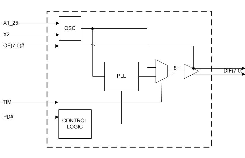
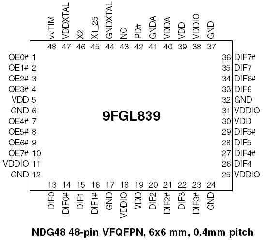
The 9FGL839 is an 8-output differential synthesizer for PCI Express Gen 1, Gen 2, and Gen 3 applications. It has integrated terminations providing direct connection to 100Ω transmission lines and saving 32 resistors compared to standard HCSL outputs. The 9FGL839 supports common, data, and Separate Reference no-Spread (SRnS) PCIe clock architectures.
特性
- Integrated terminations; save 32 resistors compared to standard HCSL outputs
- LP-HCSL outputs; support separate VDDIO rail and 130mW typical power consumption
- 8 OE# pins; hardware control of each output
- 25MHz crystal input; exact synthesis
- 100MHz operation; supports PCIe and SATA applications
- VDDIO; allows outputs to run from lower voltage rail to save power
- OE# pins have 1.5V high input threshold; direct interface to 1.8V to 3.3V systems
- < 130mW power consumption (typical)
- Cycle-to-Cycle jitter < 50ps
- Output-to-Output skew < 100ps
- PCIe Gen 2 phase jitter < 3.0ps RMS
- PCIe Gen 3 phase jitter < 1.0ps RMS
- PCIe Gen 3 SRnS clock phase jitter < 0.7ps RMS
产品对比
应用
设计和开发
模型
ECAD 模块
点击产品选项表中的 CAD 模型链接,查找 SamacSys 中的原理图符号、PCB 焊盘布局和 3D CAD 模型。如果符号和模型不可用,可直接在 SamacSys 请求该符号或模型。

产品选项
当前筛选条件
视频和培训
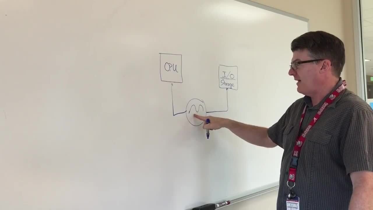
PCIe Clocking Architectures (Common and Separate)
This is the first video in our PCIe series. In this video, we define PCIe architectures, focusing on common and separate clock architectures. Watch the rest of the video series below where Ron will cover the impact of different timing architectures.
Watch the Video Series Below
Video List