概览
描述
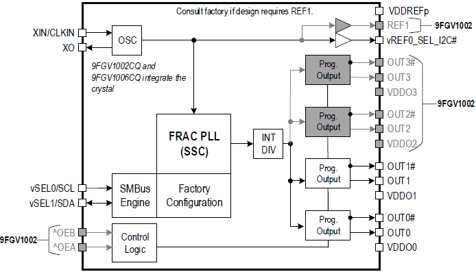
The 9FGV1006 is a member of Renesas' PhiClock™ programmable clock generator family. The 9FGV1006 provides two copies of a single integer, fractional or spread-spectrum output frequency and one copy of the crystal reference input. Two select pins allow for hardware selection of the desired configuration, or two I²C bits all easy software selection of the desired configuration. The user may configure any one of the four OTP configurations as the default when operating in I²C mode. Four unique I²C addresses are available, allowing easy I²C access to multiple components.
特性
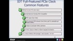
- PCIe Gen 1–7 compliant
- PCIe Gen 7 Common Clock jitter < 41fs RMS
- 276fs RMS typical phase jitter at 156.25MHz (12kHz to 20MHz)
- 2 programmable output pairs plus 1 LVCMOS REF output
- 1 integer, fractional or spread-spectrum output frequency per configuration
- 1MHz to 325MHz output frequency (LVDS or LP-HCSL)
- 1MHz to 200MHz output frequency (LVCMOS)
- 1.8V to 3.3V core VDD
- Individual 1.8V, 2.5V, or 3.3V VDDO for each programmable output pair
- Supports HCSL, LVDS, and LVCMOS I/O standards
- Supports AC-coupled LVPECL and CML logic – See AN-891
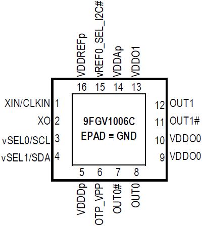
- 3mm × 3mm 16-LGA packages with 50MHz integrated crystal option
- Supported by Timing Commander™ software
产品对比
应用
设计和开发
软件与工具
开发板与套件
评估
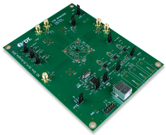
EVK9FGV1006
有效
Evaluation Kit for 9FGV1006 Programmable PhiClock™ Generator
This is the evaluation board for the 9FGV1006 programmable PhiClockTM generator. It provides a convenient way of configuring and programming the blank parts for the 9FGV1006 device. With the onboard USB interface, the Renesas Timing CommanderTM graphical user interface (GUI) can communicate with...
评估
Evaluation Kit for 9FGV1006 Programmable PhiClock™ Generator with Internal 50MHz Crystal
This is the evaluation board for the 9FGV1006Q5 programmable PhiClockTM generator with an internal 50MHz crystal. It provides a convenient way of configuring and programming the blank parts for the 9FGV1006Q5 device. With the onboard USB interface, the Renesas Timing CommanderTM graphical user...
模型
ECAD 模块
点击产品选项表中的 CAD 模型链接,查找 SamacSys 中的原理图符号、PCB 焊盘布局和 3D CAD 模型。如果符号和模型不可用,可直接在 SamacSys 请求该符号或模型。

产品选项
当前筛选条件
视频和培训
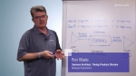
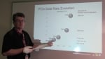
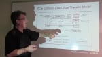
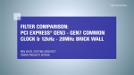
PCIe Reference Clock Jitter Budgets
Ron Wade, chief PCIe system architect explains the fundamental difference in reference clock jitter budgets between the first three generations of the specification and those of Gen4 and Gen5 which raise new challenges for designers.
Related Resources
Video List