特性
- PCIe Gen 1–7 compliant
- PCIe Gen 7 Common Clock jitter < 41fs RMS
- 276fs RMS typical phase jitter at 156.25MHz (12kHz to 20MHz)
- 2 programmable output pairs plus 1 LVCMOS REF output
- 1 integer, fractional or spread-spectrum output frequency per configuration
- 1MHz to 325MHz output frequency (LVDS or LP-HCSL)
- 1MHz to 200MHz output frequency (LVCMOS)
- 1.8V to 3.3V core VDD
- Individual 1.8V, 2.5V, or 3.3V VDDO for each programmable output pair
- Supports HCSL, LVDS, and LVCMOS I/O standards
- Supports AC-coupled LVPECL and CML logic – See AN-891
- 3mm × 3mm 16-LGA packages with 50MHz integrated crystal option
- Supported by Timing Commander™ software


描述
The 9FGV1006 is a member of Renesas' PhiClock™ programmable clock generator family. The 9FGV1006 provides two copies of a single integer, fractional or spread-spectrum output frequency and one copy of the crystal reference input. Two select pins allow for hardware selection of the desired configuration, or two I²C bits all easy software selection of the desired configuration. The user may configure any one of the four OTP configurations as the default when operating in I²C mode. Four unique I²C addresses are available, allowing easy I²C access to multiple components.
试用自定义部件配置工具。
产品参数
| 属性 | 值 |
|---|---|
| Diff. Outputs | 2 |
| Diff. Output Signaling | LP-HCSL |
| Output Freq Range (MHz) | 100 - 100 |
| Accepts Spread Spec Input | Yes |
| Power Consumption Typ (mW) | 100 |
| Supply Voltage (V) | 1.8 - 1.8, 3.3 - 3.3 |
| Output Type | LP-HCSL |
| Xtal Freq (MHz) | 25 - 25, 50 - 50 |
| Package Area (mm²) | 25 |
| Battery Backup | No |
| Battery Seal | No |
| CPU Supervisory Function POR | No |
| Crystal Frequency Trimming | No |
| Frequency Out Pin | No |
| Inputs (#) | 1 |
| Input Freq (MHz) | 25 - 25, 50 - 50 |
| Function | Generator |
| Input Type | Crystal, LVCMOS |
| Output Banks (#) | 1 |
| Core Voltage (V) | 1.8, 3.3 |
| Output Voltage (V) | 1.8, 3.3 |
| Product Category | PCI Express Clocks |
封装选项
| Pkg. Type | Pkg. Dimensions (mm) | Lead Count (#) | Pitch (mm) |
|---|---|---|---|
| LGA | 3.0 x 3.0 x 1.1 | 16 | 0.5 |
试用自定义部件配置工具。
| Part Number | Status | Samples | Longevity | Stock | Package | Budgetary Price (USD) | Lead Count (#) | Carrier Type | Moisture Sensitivity Level (MSL) | Phase Jitter Typ RMS (ps) | Core Voltage (V) | Diff. Output Signaling | Input Freq (MHz) | Output Impedance | Output Type | Output Voltage (V) | Supply Voltage (V) | Xtal Freq (MHz) | Advanced Features | App Jitter Compliance | C-C Jitter Max P-P (ps) | Input Type | Outputs (#) | Output Freq Range (MHz) | Power Consumption Typ (mW) | Prog. Clock | Qty. per Reel (#) | Qty. per Carrier (#) | Xtal Inputs (#) | Pb (Lead) Free | Pb Free Category | Temp. Range (°C) | Country of Assembly | Country of Wafer Fabrication |
|---|---|---|---|---|---|---|---|---|---|---|---|---|---|---|---|---|---|---|---|---|---|---|---|---|---|---|---|---|---|---|---|---|---|---|
| 9FGV1006C001LTGI | Active | Available | 2040 Apr | Out of Stock | LGA | 16# | Tray | 3 | 0.283ps | 3.3V | LP-HCSL | 25 - 25 | 100 | LP-HCSL | 3.3V | 3.3 - 3.3 | 25 - 25 | Programmable Clock | PCIe Gen1, PCIe Gen2, PCIe Gen3, PCIe Gen4, PCIe Gen5, PCIe Gen6, PCIe Gen7 | 50ps | Crystal, LVCMOS | 2# | 100 - 100 | 100mW | Yes | 0 | 490# | 1# | Yes | e4 Au | -40 to 85°C | |||
| 9FGV1006C001LTGI8 | Active | N/A | 2040 Apr | Out of Stock | LGA | 16# | Reel | 3 | 0.283ps | 3.3V | LP-HCSL | 25 - 25 | 100 | LP-HCSL | 3.3V | 3.3 - 3.3 | 25 - 25 | Programmable Clock | PCIe Gen1, PCIe Gen2, PCIe Gen3, PCIe Gen4, PCIe Gen5, PCIe Gen6, PCIe Gen7 | 50ps | Crystal, LVCMOS | 2# | 100 - 100 | 100mW | Yes | 3000# | 0 | 1# | Yes | e4 Au | -40 to 85°C | |||
| 9FGV1006C002LTGI | Active | Available | 2040 Apr | Out of Stock | LGA | 16# | Tray | 3 | 0.29ps | 1.8V | LP-HCSL | 25 - 25 | 100 | LP-HCSL | 1.8V | 1.8 - 1.8 | 25 - 25 | Programmable Clock | PCIe Gen1, PCIe Gen2, PCIe Gen3, PCIe Gen4, PCIe Gen5, PCIe Gen6, PCIe Gen7 | 50ps | Crystal, LVCMOS | 2# | 100 - 100 | 100mW | Yes | 0 | 490# | 1# | Yes | e4 Au | -40 to 85°C | |||
| 9FGV1006C002LTGI8 | Active | N/A | 2040 Apr | Out of Stock | LGA | 16# | Reel | 3 | 0.29ps | 1.8V | LP-HCSL | 25 - 25 | 100 | LP-HCSL | 1.8V | 1.8 - 1.8 | 25 - 25 | Programmable Clock | PCIe Gen1, PCIe Gen2, PCIe Gen3, PCIe Gen4, PCIe Gen5, PCIe Gen6, PCIe Gen7 | 50ps | Crystal, LVCMOS | 2# | 100 - 100 | 100mW | Yes | 3000# | 0 | 1# | Yes | e4 Au | -40 to 85°C | |||
| 9FGV1006C015LTGI | Active | Available | 2040 Apr | Out of Stock | LGA | 16# | Tray | 3 | 0.283ps | 3.3V | LP-HCSL | 25 - 25 | 85 | LP-HCSL | 3.3V | 3.3 - 3.3 | 25 - 25 | Programmable Clock | PCIe Gen1, PCIe Gen2, PCIe Gen3, PCIe Gen4, PCIe Gen5, PCIe Gen6, PCIe Gen7 | 50ps | Crystal, LVCMOS | 2# | 100 - 100 | 100mW | Yes | 0 | 490# | 1# | Yes | e4 Au | -40 to 85°C | |||
| 9FGV1006C015LTGI8 | Active | N/A | 2040 Apr | Out of Stock | LGA | 16# | Reel | 3 | 0.283ps | 3.3V | LP-HCSL | 25 - 25 | 85 | LP-HCSL | 3.3V | 3.3 - 3.3 | 25 - 25 | Programmable Clock | PCIe Gen1, PCIe Gen2, PCIe Gen3, PCIe Gen4, PCIe Gen5, PCIe Gen6, PCIe Gen7 | 50ps | Crystal, LVCMOS | 2# | 100 - 100 | 100mW | Yes | 3000# | 0 | 1# | Yes | e4 Au | -40 to 85°C | |||
| 9FGV1006CQ505LTGI | Active | Available | 2040 Apr | Out of Stock | LGA | 16# | Tray | 3 | 0.26ps | 3.3V | LP-HCSL | 50 - 50 | 100 | LP-HCSL | 3.3V | 3.3 - 3.3 | 50 - 50 | Programmable Clock | PCIe Gen1, PCIe Gen2, PCIe Gen3, PCIe Gen4, PCIe Gen5, PCIe Gen6, PCIe Gen7 | 50ps | Crystal, LVCMOS | 2# | 100 - 100 | 100mW | Yes | 0 | 490# | 1# | Yes | e4 Au | -40 to 85°C | |||
| 9FGV1006CQ505LTGI8 | Active | N/A | 2040 Apr | Out of Stock | LGA | 16# | Reel | 3 | 0.26ps | 3.3V | LP-HCSL | 50 - 50 | 100 | LP-HCSL | 3.3V | 3.3 - 3.3 | 50 - 50 | Programmable Clock | PCIe Gen1, PCIe Gen2, PCIe Gen3, PCIe Gen4, PCIe Gen5, PCIe Gen6, PCIe Gen7 | 50ps | Crystal, LVCMOS | 2# | 100 - 100 | 100mW | Yes | 3000# | 0 | 1# | Yes | e4 Au | -40 to 85°C | |||
| 9FGV1006CQ506LTGI | Active | Available | 2040 Apr | Out of Stock | LGA | 16# | Tray | 3 | 0.258ps | 1.8V | LP-HCSL | 50 - 50 | 100 | LP-HCSL | 1.8V | 1.8 - 1.8 | 50 - 50 | Programmable Clock | PCIe Gen1, PCIe Gen2, PCIe Gen3, PCIe Gen4, PCIe Gen5, PCIe Gen6, PCIe Gen7 | 50ps | Crystal, LVCMOS | 2# | 100 - 100 | 100mW | Yes | 0 | 490# | 1# | Yes | e4 Au | -40 to 85°C | |||
| 9FGV1006CQ506LTGI8 | Active | N/A | 2040 Apr | Out of Stock | LGA | 16# | Reel | 3 | 0.258ps | 1.8V | LP-HCSL | 50 - 50 | 100 | LP-HCSL | 1.8V | 1.8 - 1.8 | 50 - 50 | Programmable Clock | PCIe Gen1, PCIe Gen2, PCIe Gen3, PCIe Gen4, PCIe Gen5, PCIe Gen6, PCIe Gen7 | 50ps | Crystal, LVCMOS | 2# | 100 - 100 | 100mW | Yes | 3000# | 0 | 1# | Yes | e4 Au | -40 to 85°C | |||
| 9FGV1006CQ515LTGI | Active | Available | 2040 Apr | Out of Stock | LGA | 1ku | $2.74 | 16# | Tray | 3 | 0.26ps | 3.3V | LP-HCSL | 50 - 50 | 85 | LP-HCSL | 3.3V | 3.3 - 3.3 | 50 - 50 | Programmable Clock | PCIe Gen1, PCIe Gen2, PCIe Gen3, PCIe Gen4, PCIe Gen5, PCIe Gen6, PCIe Gen7 | 50ps | Crystal, LVCMOS | 2# | 100 - 100 | 100mW | Yes | 0 | 490# | 1# | Yes | e4 Au | -40 to 85°C | TAIWAN | SINGAPORE |
| 9FGV1006CQ515LTGI8 | Active | N/A | 2040 Apr | Out of Stock | LGA | 1ku | $2.74 | 16# | Reel | 3 | 0.26ps | 3.3V | LP-HCSL | 50 - 50 | 85 | LP-HCSL | 3.3V | 3.3 - 3.3 | 50 - 50 | Programmable Clock | PCIe Gen1, PCIe Gen2, PCIe Gen3, PCIe Gen4, PCIe Gen5, PCIe Gen6, PCIe Gen7 | 50ps | Crystal, LVCMOS | 2# | 100 - 100 | 100mW | Yes | 3000# | 0 | 1# | Yes | e4 Au | -40 to 85°C | TAIWAN | SINGAPORE |
| 9FGV1006A000LTGI | Obsolete | N/A | Out of Stock | LGA | 16# | Tray | 3 | 0.31ps | 1.8V, 2.5V, 3.3V | LP-HCSL, LVDS | 8 - 50 | 85, 100 | LP-HCSL, LVCMOS, LVDS | 1.8V, 2.5V, 3.3V | 1.8 - 1.8, 2.5 - 2.5, 3.3 - 3.3 | 8 - 50 | Reference Output, Spread Spectrum, Programmable Clock | PCIe Gen1, PCIe Gen2, PCIe Gen3, PCIe Gen4, PCIe Gen5 | 50ps | Crystal, LVCMOS | 3# | 10 - 325 | 100mW | No | 0 | 490# | 1# | Yes | e4 Au | -40 to 85°C | ||||
| 9FGV1006A000LTGI8 | Obsolete | N/A | Out of Stock | LGA | 16# | Reel | 3 | 0.31ps | 1.8V, 2.5V, 3.3V | LP-HCSL, LVDS | 8 - 50 | 85, 100 | LP-HCSL, LVCMOS, LVDS | 1.8V, 2.5V, 3.3V | 1.8 - 1.8, 2.5 - 2.5, 3.3 - 3.3 | 8 - 50 | Reference Output, Spread Spectrum, Programmable Clock | PCIe Gen1, PCIe Gen2, PCIe Gen3, PCIe Gen4, PCIe Gen5 | 50ps | Crystal, LVCMOS | 3# | 10 - 325 | 100mW | No | 3000# | 0 | 1# | Yes | e4 Au | -40 to 85°C | ||||
| 9FGV1006A001LTGI | Obsolete | N/A | In Stock | LGA | 16# | Tray | 3 | 0.311ps | 3.3V | LP-HCSL | 25 - 25 | 100 | LP-HCSL | 3.3V | 1.8 - 1.8, 2.5 - 2.5, 3.3 - 3.3 | 25 - 25 | Programmable Clock | PCIe Gen1, PCIe Gen2, PCIe Gen3, PCIe Gen4, PCIe Gen5 | 25ps | Crystal, LVCMOS | 2# | 100 - 100 | 125mW | No | 0 | 490# | 1# | Yes | e4 Au | -40 to 85°C | ||||
| 9FGV1006A001LTGI8 | Obsolete | N/A | Out of Stock | LGA | 16# | Reel | 3 | 0.311ps | 3.3V | LP-HCSL | 25 - 25 | 100 | LP-HCSL | 3.3V | 1.8 - 1.8, 2.5 - 2.5, 3.3 - 3.3 | 25 - 25 | Programmable Clock | PCIe Gen1, PCIe Gen2, PCIe Gen3, PCIe Gen4, PCIe Gen5 | 25ps | Crystal, LVCMOS | 2# | 100 - 100 | 125mW | No | 3000# | 0 | 1# | Yes | e4 Au | -40 to 85°C | ||||
| 9FGV1006A002LTGI | Obsolete | N/A | In Stock | LGA | 16# | Tray | 3 | 0.32ps | 1.8V | LP-HCSL | 25 - 25 | 100 | LP-HCSL | 1.8V | 1.8 - 1.8, 2.5 - 2.5, 3.3 - 3.3 | 25 - 25 | Programmable Clock | PCIe Gen1, PCIe Gen2, PCIe Gen3, PCIe Gen4, PCIe Gen5 | 25ps | Crystal, LVCMOS | 2# | 100 - 100 | 100mW | No | 0 | 490# | 1# | Yes | e4 Au | -40 to 85°C | ||||
| 9FGV1006A002LTGI8 | Obsolete | N/A | Out of Stock | LGA | 16# | Reel | 3 | 0.32ps | 1.8V | LP-HCSL | 25 - 25 | 100 | LP-HCSL | 1.8V | 1.8 - 1.8, 2.5 - 2.5, 3.3 - 3.3 | 25 - 25 | Programmable Clock | PCIe Gen1, PCIe Gen2, PCIe Gen3, PCIe Gen4, PCIe Gen5 | 25ps | Crystal, LVCMOS | 2# | 100 - 100 | 100mW | No | 3000# | 0 | 1# | Yes | e4 Au | -40 to 85°C | ||||
| 9FGV1006A003LTGI | Obsolete | N/A | Out of Stock | LGA | 16# | Tray | 3 | 0.311ps | 3.3V | LVDS | 25 - 25 | 100 | LVDS | 3.3V | 1.8 - 1.8, 2.5 - 2.5, 3.3 - 3.3 | 25 - 25 | Programmable Clock | PCIe Gen1, PCIe Gen2, PCIe Gen3, PCIe Gen4, PCIe Gen5 | 25ps | Crystal, LVCMOS | 2# | 100 - 100 | 125mW | No | 0 | 490# | 1# | Yes | e4 Au | -40 to 85°C | ||||
| 9FGV1006A003LTGI8 | Obsolete | N/A | Out of Stock | LGA | 16# | Reel | 3 | 0.311ps | 3.3V | LVDS | 25 - 25 | 100 | LVDS | 3.3V | 1.8 - 1.8, 2.5 - 2.5, 3.3 - 3.3 | 25 - 25 | Programmable Clock | PCIe Gen1, PCIe Gen2, PCIe Gen3, PCIe Gen4, PCIe Gen5 | 25ps | Crystal, LVCMOS | 2# | 100 - 100 | 125mW | No | 3000# | 0 | 1# | Yes | e4 Au | -40 to 85°C | ||||
| 9FGV1006A004LTGI | Obsolete | N/A | Out of Stock | LGA | 16# | Tray | 3 | 0.32ps | 1.8V | LVDS | 25 - 25 | 100 | LVDS | 1.8V | 1.8 - 1.8, 2.5 - 2.5, 3.3 - 3.3 | 25 - 25 | Programmable Clock | PCIe Gen1, PCIe Gen2, PCIe Gen3, PCIe Gen4, PCIe Gen5 | 25ps | Crystal, LVCMOS | 2# | 100 - 100 | 100mW | No | 0 | 490# | 1# | Yes | e4 Au | -40 to 85°C | ||||
| 9FGV1006A004LTGI8 | Obsolete | N/A | Out of Stock | LGA | 16# | Reel | 3 | 0.32ps | 1.8V | LVDS | 25 - 25 | 100 | LVDS | 1.8V | 1.8 - 1.8, 2.5 - 2.5, 3.3 - 3.3 | 25 - 25 | Programmable Clock | PCIe Gen1, PCIe Gen2, PCIe Gen3, PCIe Gen4, PCIe Gen5 | 25ps | Crystal, LVCMOS | 2# | 100 - 100 | 100mW | No | 3000# | 0 | 1# | Yes | e4 Au | -40 to 85°C | ||||
| 9FGV1006B000LTGI | Obsolete | N/A | Out of Stock | LGA | 16# | Tray | 3 | 0.276ps | 1.8V, 2.5V, 3.3V | LP-HCSL, LVDS | 8 - 50 | 85, 100 | LP-HCSL, LVCMOS, LVDS | 1.8V, 2.5V, 3.3V | 1.8 - 1.8, 2.5 - 2.5, 3.3 - 3.3 | 8 - 50 | Reference Output, Spread Spectrum, Programmable Clock | PCIe Gen1, PCIe Gen2, PCIe Gen3, PCIe Gen4, PCIe Gen5 | 50ps | Crystal, LVCMOS | 3# | 10 - 325 | 100mW | No | 0 | 490# | 1# | Yes | e4 Au | -40 to 85°C | ||||
| 9FGV1006B000LTGI8 | Obsolete | N/A | Out of Stock | LGA | 16# | Reel | 3 | 0.276ps | 1.8V, 2.5V, 3.3V | LP-HCSL, LVDS | 8 - 50 | 85, 100 | LP-HCSL, LVCMOS, LVDS | 1.8V, 2.5V, 3.3V | 1.8 - 1.8, 2.5 - 2.5, 3.3 - 3.3 | 8 - 50 | Reference Output, Spread Spectrum, Programmable Clock | PCIe Gen1, PCIe Gen2, PCIe Gen3, PCIe Gen4, PCIe Gen5 | 50ps | Crystal, LVCMOS | 3# | 10 - 325 | 100mW | No | 3000# | 0 | 1# | Yes | e4 Au | -40 to 85°C | ||||
| 9FGV1006B001LTGI | Obsolete | N/A | In Stock | LGA | 16# | Tray | 3 | 0.276ps | 3.3V | LP-HCSL, LVDS | 8 - 50 | 100 | LP-HCSL, LVCMOS, LVDS | 1.8V, 2.5V, 3.3V | 1.8 - 1.8, 2.5 - 2.5, 3.3 - 3.3 | Reference Output, Spread Spectrum, Programmable Clock | PCIe Gen1, PCIe Gen2, PCIe Gen3, PCIe Gen4, PCIe Gen5 | 50ps | Crystal, LVCMOS | 3# | 10 - 325 | 100mW | No | 0 | 490# | 1# | Yes | e4 Au | -40 to 85°C | |||||
| 9FGV1006B001LTGI8 | Obsolete | N/A | Out of Stock | LGA | 16# | Reel | 3 | 0.276ps | 3.3V | LP-HCSL, LVDS | 8 - 50 | 100 | LP-HCSL, LVCMOS, LVDS | 1.8V, 2.5V, 3.3V | 1.8 - 1.8, 2.5 - 2.5, 3.3 - 3.3 | Reference Output, Spread Spectrum, Programmable Clock | PCIe Gen1, PCIe Gen2, PCIe Gen3, PCIe Gen4, PCIe Gen5 | 50ps | Crystal, LVCMOS | 3# | 10 - 325 | 100mW | No | 3000# | 0 | 1# | Yes | e4 Au | -40 to 85°C | |||||
| 9FGV1006B002LTGI | Obsolete | N/A | In Stock | LGA | 16# | Tray | 3 | 0.276ps | 1.8V | LP-HCSL, LVDS | 8 - 50 | 100 | LP-HCSL, LVCMOS, LVDS | 1.8V, 2.5V, 3.3V | 1.8 - 1.8, 2.5 - 2.5, 3.3 - 3.3 | Reference Output, Spread Spectrum, Programmable Clock | PCIe Gen1, PCIe Gen2, PCIe Gen3, PCIe Gen4, PCIe Gen5 | 50ps | Crystal, LVCMOS | 3# | 10 - 325 | 100mW | No | 0 | 490# | 1# | Yes | e4 Au | -40 to 85°C | |||||
| 9FGV1006B002LTGI8 | Obsolete | N/A | Out of Stock | LGA | 16# | Reel | 3 | 0.276ps | 1.8V | LP-HCSL, LVDS | 8 - 50 | 100 | LP-HCSL, LVCMOS, LVDS | 1.8V, 2.5V, 3.3V | 1.8 - 1.8, 2.5 - 2.5, 3.3 - 3.3 | Reference Output, Spread Spectrum, Programmable Clock | PCIe Gen1, PCIe Gen2, PCIe Gen3, PCIe Gen4, PCIe Gen5 | 50ps | Crystal, LVCMOS | 3# | 10 - 325 | 100mW | No | 3000# | 0 | 1# | Yes | e4 Au | -40 to 85°C | |||||
| 9FGV1006B015LTGI | Obsolete | N/A | Out of Stock | LGA | 16# | Tray | 3 | 0.276ps | 3.3V | LP-HCSL, LVDS | 8 - 50 | 85 | LP-HCSL, LVCMOS, LVDS | 1.8V, 2.5V, 3.3V | 1.8 - 1.8, 2.5 - 2.5, 3.3 - 3.3 | Reference Output, Spread Spectrum, Programmable Clock | PCIe Gen1, PCIe Gen2, PCIe Gen3, PCIe Gen4, PCIe Gen5 | 50ps | Crystal, LVCMOS | 3# | 10 - 325 | 100mW | No | 0 | 490# | 1# | Yes | e4 Au | -40 to 85°C | |||||
| 9FGV1006B015LTGI8 | Obsolete | N/A | Out of Stock | LGA | 16# | Reel | 3 | 0.276ps | 3.3V | LP-HCSL, LVDS | 8 - 50 | 85 | LP-HCSL, LVCMOS, LVDS | 1.8V, 2.5V, 3.3V | 1.8 - 1.8, 2.5 - 2.5, 3.3 - 3.3 | Reference Output, Spread Spectrum, Programmable Clock | PCIe Gen1, PCIe Gen2, PCIe Gen3, PCIe Gen4, PCIe Gen5 | 50ps | Crystal, LVCMOS | 3# | 10 - 325 | 100mW | No | 3000# | 0 | 1# | Yes | e4 Au | -40 to 85°C | |||||
| 9FGV1006BQ500LTGI | Obsolete | N/A | Out of Stock | LGA | 16# | Tray | 3 | 0.276ps | 1.8V, 2.5V, 3.3V | LP-HCSL, LVDS | 8 - 50 | 85, 100 | LP-HCSL, LVCMOS, LVDS | 1.8V, 2.5V, 3.3V | 1.8 - 1.8, 2.5 - 2.5, 3.3 - 3.3 | 8 - 50 | Reference Output, Spread Spectrum, Programmable Clock | PCIe Gen1, PCIe Gen2, PCIe Gen3, PCIe Gen4, PCIe Gen5 | 50ps | Crystal, LVCMOS | 3# | 10 - 325 | 100mW | No | 0 | 490# | 1# | Yes | e4 Au | -40 to 85°C | ||||
| 9FGV1006BQ500LTGI8 | Obsolete | N/A | Out of Stock | LGA | 16# | Reel | 3 | 0.276ps | 1.8V, 2.5V, 3.3V | LP-HCSL, LVDS | 8 - 50 | 85, 100 | LP-HCSL, LVCMOS, LVDS | 1.8V, 2.5V, 3.3V | 1.8 - 1.8, 2.5 - 2.5, 3.3 - 3.3 | 8 - 50 | Reference Output, Spread Spectrum, Programmable Clock | PCIe Gen1, PCIe Gen2, PCIe Gen3, PCIe Gen4, PCIe Gen5 | 50ps | Crystal, LVCMOS | 3# | 10 - 325 | 100mW | No | 3000# | 0 | 1# | Yes | e4 Au | -40 to 85°C | ||||
| 9FGV1006BQ505LTGI | Obsolete | N/A | Out of Stock | LGA | 16# | Tray | 3 | 0.276ps | 3.3V | LP-HCSL, LVDS | 8 - 50 | 100 | LP-HCSL, LVCMOS, LVDS | 1.8V, 2.5V, 3.3V | 1.8 - 1.8, 2.5 - 2.5, 3.3 - 3.3 | Reference Output, Spread Spectrum, Programmable Clock | PCIe Gen1, PCIe Gen2, PCIe Gen3, PCIe Gen4, PCIe Gen5 | 50ps | Crystal, LVCMOS | 3# | 10 - 325 | 100mW | No | 0 | 490# | 1# | Yes | e4 Au | -40 to 85°C | |||||
| 9FGV1006BQ505LTGI8 | Obsolete | N/A | Out of Stock | LGA | 16# | Reel | 3 | 0.276ps | 3.3V | LP-HCSL, LVDS | 8 - 50 | 100 | LP-HCSL, LVCMOS, LVDS | 1.8V, 2.5V, 3.3V | 1.8 - 1.8, 2.5 - 2.5, 3.3 - 3.3 | Reference Output, Spread Spectrum, Programmable Clock | PCIe Gen1, PCIe Gen2, PCIe Gen3, PCIe Gen4, PCIe Gen5 | 50ps | Crystal, LVCMOS | 3# | 10 - 325 | 100mW | No | 3000# | 0 | 1# | Yes | e4 Au | -40 to 85°C | |||||
| 9FGV1006BQ506LTGI | Obsolete | N/A | Out of Stock | LGA | 16# | Tray | 3 | 0.276ps | 1.8V | LP-HCSL, LVDS | 8 - 50 | 100 | LP-HCSL, LVCMOS, LVDS | 1.8V, 2.5V, 3.3V | 1.8 - 1.8, 2.5 - 2.5, 3.3 - 3.3 | Reference Output, Spread Spectrum, Programmable Clock | PCIe Gen1, PCIe Gen2, PCIe Gen3, PCIe Gen4, PCIe Gen5 | 50ps | Crystal, LVCMOS | 3# | 10 - 325 | 100mW | No | 0 | 490# | 1# | Yes | e4 Au | -40 to 85°C | |||||
| 9FGV1006BQ506LTGI8 | Obsolete | N/A | Out of Stock | LGA | 16# | Reel | 3 | 0.276ps | 1.8V | LP-HCSL, LVDS | 8 - 50 | 100 | LP-HCSL, LVCMOS, LVDS | 1.8V, 2.5V, 3.3V | 1.8 - 1.8, 2.5 - 2.5, 3.3 - 3.3 | Reference Output, Spread Spectrum, Programmable Clock | PCIe Gen1, PCIe Gen2, PCIe Gen3, PCIe Gen4, PCIe Gen5 | 50ps | Crystal, LVCMOS | 3# | 10 - 325 | 100mW | No | 3000# | 0 | 1# | Yes | e4 Au | -40 to 85°C | |||||
| 9FGV1006BQ515LTGI | Obsolete | N/A | Out of Stock | LGA | 16# | Tray | 3 | 0.276ps | 3.3V | LP-HCSL, LVDS | 8 - 50 | 85 | LP-HCSL, LVCMOS, LVDS | 1.8V, 2.5V, 3.3V | 1.8 - 1.8, 2.5 - 2.5, 3.3 - 3.3 | Reference Output, Spread Spectrum, Programmable Clock | PCIe Gen1, PCIe Gen2, PCIe Gen3, PCIe Gen4, PCIe Gen5 | 50ps | Crystal, LVCMOS | 3# | 10 - 325 | 100mW | No | 0 | 490# | 1# | Yes | e4 Au | -40 to 85°C | |||||
| 9FGV1006BQ515LTGI8 | Obsolete | N/A | Out of Stock | LGA | 16# | Reel | 3 | 0.276ps | 3.3V | LP-HCSL, LVDS | 8 - 50 | 85 | LP-HCSL, LVCMOS, LVDS | 1.8V, 2.5V, 3.3V | 1.8 - 1.8, 2.5 - 2.5, 3.3 - 3.3 | Reference Output, Spread Spectrum, Programmable Clock | PCIe Gen1, PCIe Gen2, PCIe Gen3, PCIe Gen4, PCIe Gen5 | 50ps | Crystal, LVCMOS | 3# | 10 - 325 | 100mW | No | 3000# | 0 | 1# | Yes | e4 Au | -40 to 85°C | |||||
| 9FGV1006Q500LTGI | Obsolete | N/A | Out of Stock | LGA | 16# | Tray | 3 | 0.31ps | 1.8V, 2.5V, 3.3V | LP-HCSL, LVDS | 8 - 50 | 85, 100 | LP-HCSL, LVCMOS, LVDS | 1.8V, 2.5V, 3.3V | 1.8 - 1.8, 2.5 - 2.5, 3.3 - 3.3 | 50 - 50 | Reference Output, Spread Spectrum, Programmable Clock | PCIe Gen1, PCIe Gen2, PCIe Gen3, PCIe Gen4, PCIe Gen5 | 50ps | Crystal, LVCMOS | 3# | 10 - 325 | 100mW | No | 0 | 490# | 1# | Yes | e4 Au | -40 to 85°C | ||||
| 9FGV1006Q500LTGI8 | Obsolete | N/A | Out of Stock | LGA | 16# | Reel | 3 | 0.31ps | 1.8V, 2.5V, 3.3V | LP-HCSL, LVDS | 8 - 50 | 85, 100 | LP-HCSL, LVCMOS, LVDS | 1.8V, 2.5V, 3.3V | 1.8 - 1.8, 2.5 - 2.5, 3.3 - 3.3 | 50 - 50 | Reference Output, Spread Spectrum, Programmable Clock | PCIe Gen1, PCIe Gen2, PCIe Gen3, PCIe Gen4, PCIe Gen5 | 50ps | Crystal, LVCMOS | 3# | 10 - 325 | 100mW | No | 3000# | 0 | 1# | Yes | e4 Au | -40 to 85°C | ||||
| 9FGV1006Q505LTGI | Obsolete | N/A | Out of Stock | LGA | 16# | Tray | 3 | 0.296ps | 3.3V | LP-HCSL | 50 - 50 | 100 | LP-HCSL | 3.3V | 1.8 - 1.8, 2.5 - 2.5, 3.3 - 3.3 | 50 - 50 | Programmable Clock | PCIe Gen1, PCIe Gen2, PCIe Gen3, PCIe Gen4, PCIe Gen5 | 50ps | Crystal (integrated) | 2# | 100 - 100 | 125mW | No | 0 | 490# | 0 | Yes | e4 Au | -40 to 85°C | ||||
| 9FGV1006Q505LTGI8 | Obsolete | N/A | Out of Stock | LGA | 16# | Reel | 3 | 0.296ps | 3.3V | LP-HCSL | 50 - 50 | 100 | LP-HCSL | 3.3V | 1.8 - 1.8, 2.5 - 2.5, 3.3 - 3.3 | 50 - 50 | Programmable Clock | PCIe Gen1, PCIe Gen2, PCIe Gen3, PCIe Gen4, PCIe Gen5 | 50ps | Crystal (integrated) | 2# | 100 - 100 | 125mW | No | 3000# | 0 | 0 | Yes | e4 Au | -40 to 85°C | ||||
| 9FGV1006Q506LTGI | NRND | Available | Out of Stock | LGA | 16# | Tray | 3 | 0.305ps | 1.8V | LP-HCSL | 50 - 50 | 100 | LP-HCSL | 1.8V | 1.8 - 1.8, 2.5 - 2.5, 3.3 - 3.3 | 50 - 50 | Programmable Clock | PCIe Gen1, PCIe Gen2, PCIe Gen3, PCIe Gen4, PCIe Gen5 | 50ps | Crystal (integrated) | 2# | 100 - 100 | 100mW | No | 0 | 490# | 0 | Yes | e4 Au | -40 to 85°C | ||||
| 9FGV1006Q506LTGI8 | NRND | N/A | Out of Stock | LGA | 16# | Reel | 3 | 0.305ps | 1.8V | LP-HCSL | 50 - 50 | 100 | LP-HCSL | 1.8V | 1.8 - 1.8, 2.5 - 2.5, 3.3 - 3.3 | 50 - 50 | Programmable Clock | PCIe Gen1, PCIe Gen2, PCIe Gen3, PCIe Gen4, PCIe Gen5 | 50ps | Crystal (integrated) | 2# | 100 - 100 | 100mW | No | 3000# | 0 | 0 | Yes | e4 Au | -40 to 85°C | ||||
| 9FGV1006Q507LTGI | Obsolete | N/A | Out of Stock | LGA | 16# | Tray | 3 | 0.296ps | 3.3V | LVDS | 50 - 50 | 100 | LVDS | 3.3V | 1.8 - 1.8, 2.5 - 2.5, 3.3 - 3.3 | 50 - 50 | Programmable Clock | PCIe Gen1, PCIe Gen2, PCIe Gen3, PCIe Gen4, PCIe Gen5 | 50ps | Crystal (integrated) | 2# | 100 - 100 | 125mW | No | 0 | 490# | 0 | Yes | e4 Au | -40 to 85°C | ||||
| 9FGV1006Q507LTGI8 | Obsolete | N/A | Out of Stock | LGA | 16# | Reel | 3 | 0.296ps | 3.3V | LVDS | 50 - 50 | 100 | LVDS | 3.3V | 1.8 - 1.8, 2.5 - 2.5, 3.3 - 3.3 | 50 - 50 | Programmable Clock | PCIe Gen1, PCIe Gen2, PCIe Gen3, PCIe Gen4, PCIe Gen5 | 50ps | Crystal (integrated) | 2# | 100 - 100 | 125mW | No | 3000# | 0 | 0 | Yes | e4 Au | -40 to 85°C | ||||
| 9FGV1006Q508LTGI | Obsolete | N/A | Out of Stock | LGA | 16# | Tray | 3 | 0.305ps | 1.8V | LVDS | 50 - 50 | 100 | LVDS | 1.8V | 1.8 - 1.8, 2.5 - 2.5, 3.3 - 3.3 | 50 - 50 | Programmable Clock | PCIe Gen1, PCIe Gen2, PCIe Gen3, PCIe Gen4, PCIe Gen5 | 50ps | Crystal (integrated) | 2# | 100 - 100 | 100mW | No | 0 | 490# | 0 | Yes | e4 Au | -40 to 85°C | ||||
| 9FGV1006Q508LTGI8 | Obsolete | N/A | Out of Stock | LGA | 16# | Reel | 3 | 0.305ps | 1.8V | LVDS | 50 - 50 | 100 | LVDS | 1.8V | 1.8 - 1.8, 2.5 - 2.5, 3.3 - 3.3 | 50 - 50 | Programmable Clock | PCIe Gen1, PCIe Gen2, PCIe Gen3, PCIe Gen4, PCIe Gen5 | 50ps | Crystal (integrated) | 2# | 100 - 100 | 100mW | No | 3000# | 0 | 0 | Yes | e4 Au | -40 to 85°C |
- 应用说明英语PDF 1.53 MB R31AN0034EU0102 Rev.1.02 2025年10月21日AI 生成的摘要: PLL loop filter design involves selecting component values to ensure stable operation and optimized phase noise. The loop bandwidth depends on parameters like charge pump current, VCO gain, and feedback divider. Second and third order passive loop filters are common, with specific calculations for cutoff, zero, and pole frequencies guiding component selection. Proper tuning of loop bandwidth enhances PLL stability and phase noise performance, demonstrated through lab experiments and calculation examples.
- 应用说明英语PDF 431 KB 7WDXRDKU4E7E-5-59216 2023年12月06日
- 应用说明英语PDF 256 KB 2021年7月05日AI 生成的摘要: The document explains methods to generate a 1.2V LVCMOS signal from a 1.8V LVCMOS output by attenuating the amplitude without lowering the driver voltage. It details typical LVCMOS driver and receiver configurations, impedance matching using source termination, and the use of a parallel resistor at the receiver input to reduce signal amplitude. Simulation and measurement results demonstrate that adding a parallel resistor effectively lowers the voltage to 1.2V while maintaining signal integrity and minimal impact on jitter and frequency. This approach supports flexible amplitude adjustment for various low-voltage LVCMOS requirements in clock signal applications.
推荐文档 (1)
数据手册 (7)
- 手册 - 软件英语PDF 323 KB 7WDXRDKU4E7E-5-62422 2018年2月23日
- 手册 - 软件英语PDF 401 KB 7WDXRDKU4E7E-5-62508 2017年11月27日
手册和指南 (3)
- 应用说明英语PDF 1.53 MB R31AN0034EU0102 Rev.1.02 2025年10月21日AI 生成的摘要: PLL loop filter design involves selecting component values to ensure stable operation and optimized phase noise. The loop bandwidth depends on parameters like charge pump current, VCO gain, and feedback divider. Second and third order passive loop filters are common, with specific calculations for cutoff, zero, and pole frequencies guiding component selection. Proper tuning of loop bandwidth enhances PLL stability and phase noise performance, demonstrated through lab experiments and calculation examples.
- 应用说明英语PDF 431 KB 7WDXRDKU4E7E-5-59216 2023年12月06日
- 应用说明英语PDF 256 KB 2021年7月05日AI 生成的摘要: The document explains methods to generate a 1.2V LVCMOS signal from a 1.8V LVCMOS output by attenuating the amplitude without lowering the driver voltage. It details typical LVCMOS driver and receiver configurations, impedance matching using source termination, and the use of a parallel resistor at the receiver input to reduce signal amplitude. Simulation and measurement results demonstrate that adding a parallel resistor effectively lowers the voltage to 1.2V while maintaining signal integrity and minimal impact on jitter and frequency. This approach supports flexible amplitude adjustment for various low-voltage LVCMOS requirements in clock signal applications.查看更多 (21)
应用说明和白皮书 (21)
- 产品变更通告英语PDF 761 KB 7WDXRDKU4E7E-5-63278 2018年9月25日
产品通告(产品变更、EOL 等) (3)
No Results Found.
确保所有关键词拼写正确。
尝试使用更少、不同或更宽泛的词语来改变搜索结果。
如果您使用了筛选器,请考虑取消选择某些筛选器选项以扩大搜索结果。
- 搜索我们丰富的知识库,帮助您解答常见问题
- 前往支持论坛,获取瑞萨电子技术专家和社群的帮助
No Results Found.
确保所有关键词拼写正确。
尝试使用更少、不同或更宽泛的词语来改变搜索结果。
如果您使用了筛选器,请考虑取消选择某些筛选器选项以扩大搜索结果。
- 搜索我们丰富的知识库,帮助您解答常见问题
- 前往支持论坛,获取瑞萨电子技术专家和社群的帮助
原理图和设计文件 (1)
No Results Found.
确保所有关键词拼写正确。
尝试使用更少、不同或更宽泛的词语来改变搜索结果。
如果您使用了筛选器,请考虑取消选择某些筛选器选项以扩大搜索结果。
- 搜索我们丰富的知识库,帮助您解答常见问题
- 前往支持论坛,获取瑞萨电子技术专家和社群的帮助
No Results Found.
确保所有关键词拼写正确。
尝试使用更少、不同或更宽泛的词语来改变搜索结果。
如果您使用了筛选器,请考虑取消选择某些筛选器选项以扩大搜索结果。
- 搜索我们丰富的知识库,帮助您解答常见问题
- 前往支持论坛,获取瑞萨电子技术专家和社群的帮助
No Results Found.
确保所有关键词拼写正确。
尝试使用更少、不同或更宽泛的词语来改变搜索结果。
如果您使用了筛选器,请考虑取消选择某些筛选器选项以扩大搜索结果。
- 搜索我们丰富的知识库,帮助您解答常见问题
- 前往支持论坛,获取瑞萨电子技术专家和社群的帮助
营销资料 (1)
其他 (1)
No Results Found.
确保所有关键词拼写正确。
尝试使用更少、不同或更宽泛的词语来改变搜索结果。
如果您使用了筛选器,请考虑取消选择某些筛选器选项以扩大搜索结果。
- 搜索我们丰富的知识库,帮助您解答常见问题
- 前往支持论坛,获取瑞萨电子技术专家和社群的帮助
No Results Found.
确保所有关键词拼写正确。
尝试使用更少、不同或更宽泛的词语来改变搜索结果。
如果您使用了筛选器,请考虑取消选择某些筛选器选项以扩大搜索结果。
- 搜索我们丰富的知识库,帮助您解答常见问题
- 前往支持论坛,获取瑞萨电子技术专家和社群的帮助
Renesas Boards & Kits
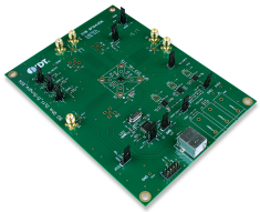
Evaluation Kit for 9FGV1006 Programmable PhiClock™ Generator
This is the evaluation board for the 9FGV1006 programmable PhiClockTM generator. It provides a convenient way of configuring and programming the blank parts for the 9FGV1006 device. With the onboard USB interface, the Renesas Timing CommanderTM graphical user interface (GUI) can communicate with... 阅读详情
Evaluation Kit for 9FGV1006 Programmable PhiClock™ Generator with Internal 50MHz Crystal
This is the evaluation board for the 9FGV1006Q5 programmable PhiClockTM generator with an internal 50MHz crystal. It provides a convenient way of configuring and programming the blank parts for the 9FGV1006Q5 device. With the onboard USB interface, the Renesas Timing CommanderTM graphical user... 阅读详情
