特性
- Device clock domain (RF-PLL) with support for JESD204B/C
- Digital clock domain (Ethernet, FEC) with support for eEEC and T-BC/T-TSC Class C
- 2 differential clock reference inputs with 1PPS (1Hz) to 1GHz input frequency
- Dual DPLL front-end with independent clock paths
- External control of the DCO for IEEE1588
- Digital holdover with a 1.1 × 10⁻⁷ ppb accuracy
- Programmable DPLL loop bandwidth 1mHz - 6kHz
- Configurable phase delay (range: 1UI)
- Hitless input switching with < 1ns output phase error
- Reference monitors for input LOS, activity and frequency
- 1 external synchronization input for JESD204B/C (LVCMOS)
- 16 differential outputs
- Optimized for low phase noise: -146dBc/Hz (1MHz offset; 245.76MHz clock)
- Supply voltage (core): 3.3V; (outputs): 3.3V, 2.5V, and 1.8V
- Board temperature range: -40°C to +105°C
- Applicable Standards
- ITU-T G.8262 EEC1/2, G.8262.1 eEEC
- ITU-T G.8273.2 T-BC/T-TSC Class C
- JESD204B and C


描述
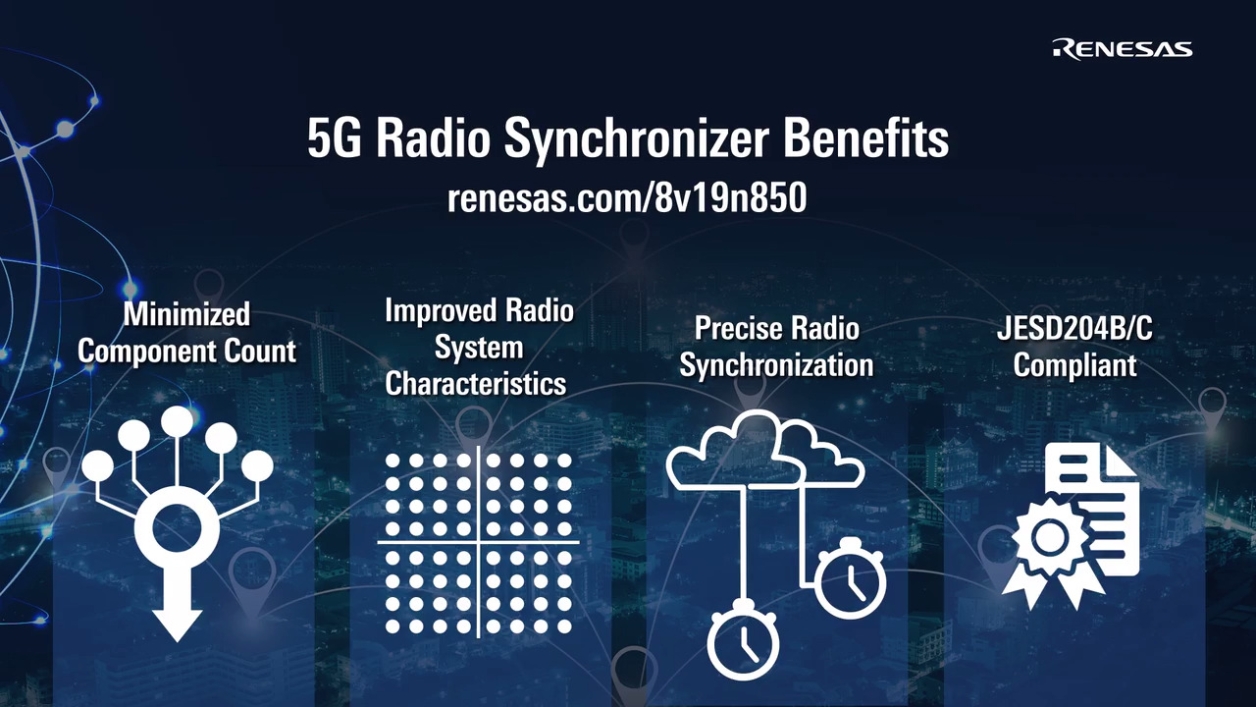
The 8V19N850 is a fully integrated Radio Unit Clock Synchronizer and Jitter Attenuator designed as a high-performance clock solution for phase/frequency synchronization and signal conditioning of wireless base station radio equipment. The device supports JESD204B/C subclass 0 and 1 device clocks and SYSREF synchronization for converters. The 8V19N850 supports two independent frequency domains: one that can be used for the digital clock (Ethernet and FEC rates) domain with four outputs, and the device clock (RF-PLL) domain with 12 outputs. The Ethernet domain generates frequencies from two independent APLLs for flexibility; the outputs of the RF clock domain generate very low phase noise clocks for ADC/DAC circuits.
From the integrated RF-PLL, the device supports the clock generation of high-frequency device clocks for driving ADC/DAC devices low-frequency synchronization signals (SYSREF). A dual DPLL front-end architecture supports any frequency translation. Each DPLL provides a programmable bandwidth and a DCO function for real-time frequency/phase adjustments. The DPLLs can lock on 1PPS input signals and establish lock within 100s or less. Frequency information can be applied from DPLL-0 to DPLL-1 and vice versa to enable the combining of the frequency characteristics of two references (combo-mode). The 8V19N850 is configured through a pin-mapped I3C (including legacy I2C) and 3/4-wire SPI interface. I2C with master capabilities reads a default configuration from an external ROM device. GPIO ports can be configured for reporting and controlling purposes.
产品参数
| 属性 | 值 |
|---|---|
| Temp. Range (°C) | -40 to 85°C |
封装选项
| Pkg. Type | Pkg. Dimensions (mm) | Lead Count (#) | Pitch (mm) |
|---|---|---|---|
| VFQFPN | 10.0 x 10.0 x 0.9 | 88 | 0.4 |
应用
- Wireless infrastructure 5G radio
This video introduces the industry’s first fully-integrated synchronizer for 5G enhanced common public radio interface (eCPRI) radio synchronization.