概览
描述
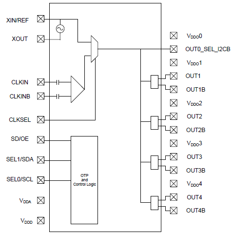
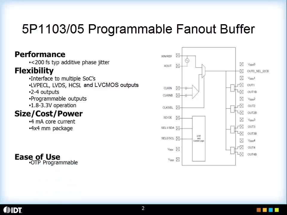
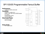
The 5P1105 is a programmable fanout buffer intended for high-performance consumer, networking, industrial, computing, and data communications applications. Configurations may be stored in on-chip One-Time Programmable (OTP) memory or changed using the I²C interface.
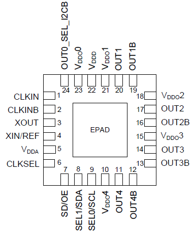
The outputs are generated from a single reference clock. The reference clock can come from one of the two redundant clock inputs. A glitchless manual switchover function allows one of the redundant clocks to be selected during normal operation. Two select pins allow up to four different configurations to be programmed and accessible using processor GPIOs or bootstrapping. The device is available in a 24-pin VFQFPN 4mm x 4mm package, with an industrial operating temperature range of -40 °C to +85 °C.
特性
- Up to four high-performance universal differential output pairs:
- Low RMS additive phase jitter: 0.2ps
- Four banks of internal non-volatile in-system programmable or factory programmable OTP memory
- I²C serial programming interface
- One additional LVCMOS output clock
- Four universal output pairs:
- Each configurable as one differential output pair or two LVCMOS outputs
- I/O standards:
- Single-ended I/Os: 1.8V to 3.3V LVCMOS
- Differential I/Os: LVPECL, LVDS, and HCSL
- Input frequency ranges:
- LVCMOS reference clock input (XIN/REF) – 1MHz to 200MHz
- LVDS, LVPECL, HCSL differential clock input (CLKIN, CLKINB) – 1MHz to 350MHz
- Crystal frequency range – 8MHz to 40MHz
- Individually selectable output voltage (1.8V, 2.5V, 3.3V) for each output pair
- Redundant clock inputs with manual switchover
- Programmable crystal load capacitance
- Individual output enable/disable
- Power-down mode
- 1.8V, 2.5V, or 3.3V core VDDD, VDDA
产品对比
应用
设计和开发
软件与工具
软件与工具
| Software title
|
Software type
|
公司
|
|---|---|---|
| Timing Commander Timing Commander™ 是一个基于 Windows™ 的创新软件平台,通过这个平台,系统设计工程师可以通过直观且灵活的图形用户界面 (GUI) 对精密的计时设备进行配置、编程和监控。
|
Code Generator | 瑞萨电子 |
1 item
|
||
开发板与套件
评估
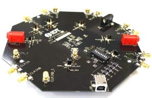
EVK-5P1105
有效
Evaluation Board for 5P1105 Universal Output Buffer
Renesas 5P1105 Programmable buffer outputs can be individually programmed as LVDS, LVPECL, HCSL, or two LVCMOS outputs per output pair, with a crystal, LVCMOS, or differential input. There are up to four universal output pairs, as well as an LVCMOS output clock. Output frequencies range from 1...
模型
ECAD 模块
点击产品选项表中的 CAD 模型链接,查找 SamacSys 中的原理图符号、PCB 焊盘布局和 3D CAD 模型。如果符号和模型不可用,可直接在 SamacSys 请求该符号或模型。

产品选项
当前筛选条件
视频和培训

新闻和博客
新闻
2015年5月1日
|