概览
描述
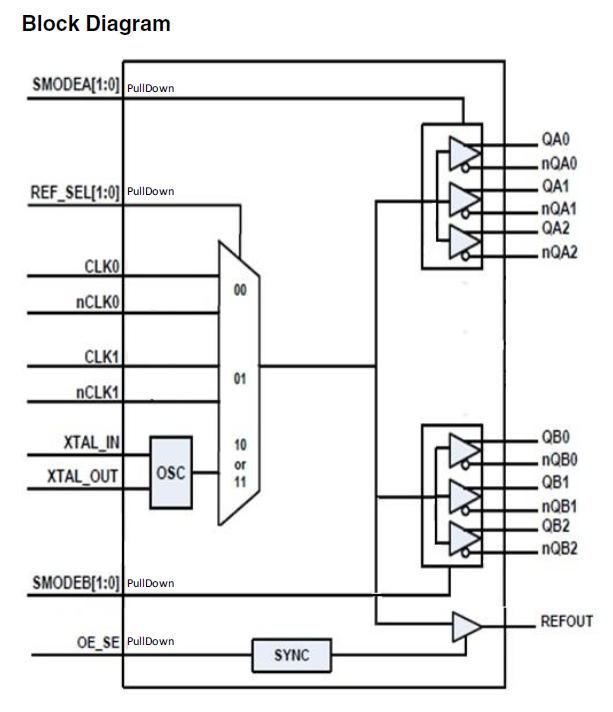
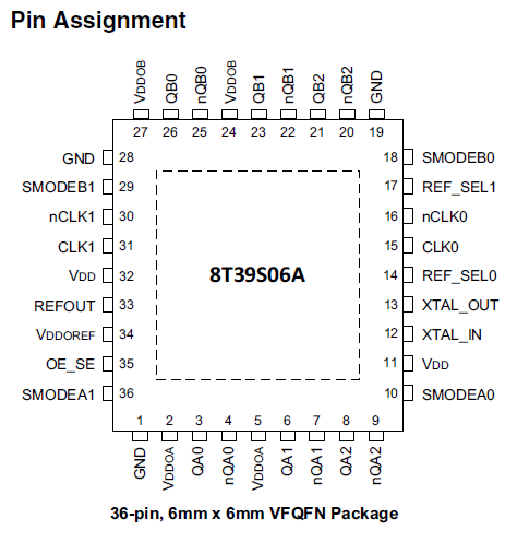
The 8T39S06A is a high-performance clock fanout buffer. The input clock can be selected from two differential inputs or one crystal input. The internal oscillator circuit is automatically disabled if the crystal input is not selected. The crystal pin can be driven by a single-ended clock. The selected signal is distributed to six differential outputs which can be configured as LVPECL, LVDS, or HCSL outputs. In addition, an LVCMOS output is provided. All outputs can be disabled into a high-impedance state. The device is designed for a signal fanout of high-frequency, low phase-noise clock and data signal. The outputs are at a defined level when inputs are open or tied to ground. It is designed to operate from a 3.3V or 2.5V core power supply, and either a 3.3V or 2.5V output operating supply.
特性
- Two differential reference clock input pairs
- Differential input pairs can accept the following input levels: LVPECL, LVDS, HCSL, HSTL, and single-ended
- Crystal oscillator interface
- Crystal input frequency range: 10MHz to 40MHz
- Maximum output frequency
LVPECL - 2GHz
LVDS - 2GHz
HCSL - 250MHz
LVCMOS - 250MHz - Two banks, each has three differential output pairs that can be configured as LVPECL, LVDS, or HCSL
- One single-ended reference output with synchronous enable to avoid clock glitch
- Output skew: 80ps (maximum)
(Bank A and Bank B at the same output level) - Part-to-part skew: 200ps (typical)
- Additive RMS phase jitter at 156.25MHz, (12kHz to 20MHz): 34.7fs (typical), 3.3V/3.3V
- Supply voltage modes:
VDD/VDDO
3.3V/3.3V
3.3V/2.5V
2.5V/2.5V - -40 °C to 85 °C ambient operating temperature
- Lead-free (RoHS 6) packaging
产品对比
应用
设计和开发

产品选项
当前筛选条件
视频和培训
新闻和博客
博客
2018年12月15日
|