特性
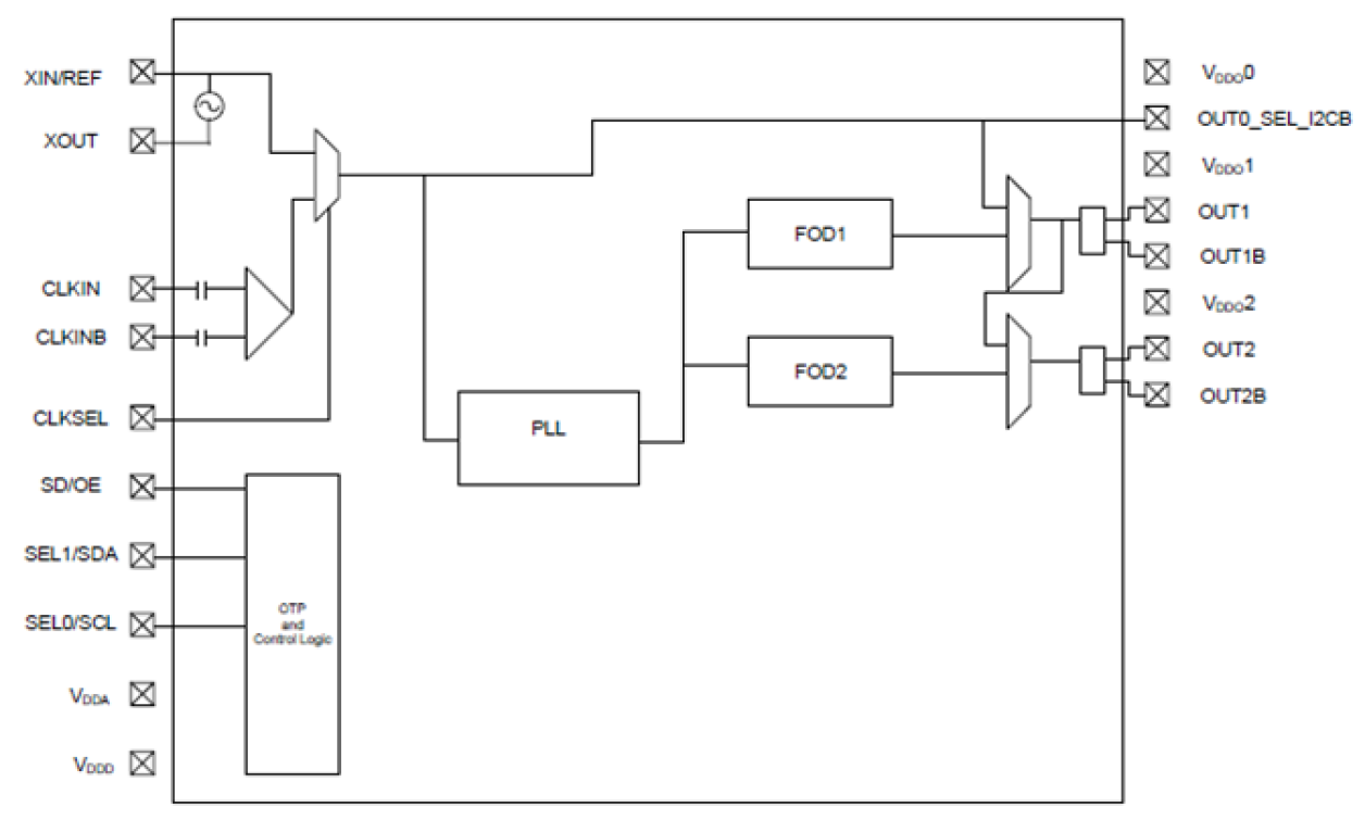
- 2 differential outputs LVPECL, LVDS, HCSL - or 4 LVCMOS outputs
- 1 additional LVCMOS output
- In-system programmable with 2 independent output frequencies
- Up to 350 MHz input/output frequencies
- Also supports crystal input
- Stores 4 different configurations in OTP non-volatile memory
- < 100 mW core power (at 3.3V)
- < 0.7 ps RMS phase jitter (typ)
- Meets PCIe® Gen1/2/3, USB 3.0, 1/10 GbE clock requirements
- 1.8 / 2.5 / 3.3V core and output voltages
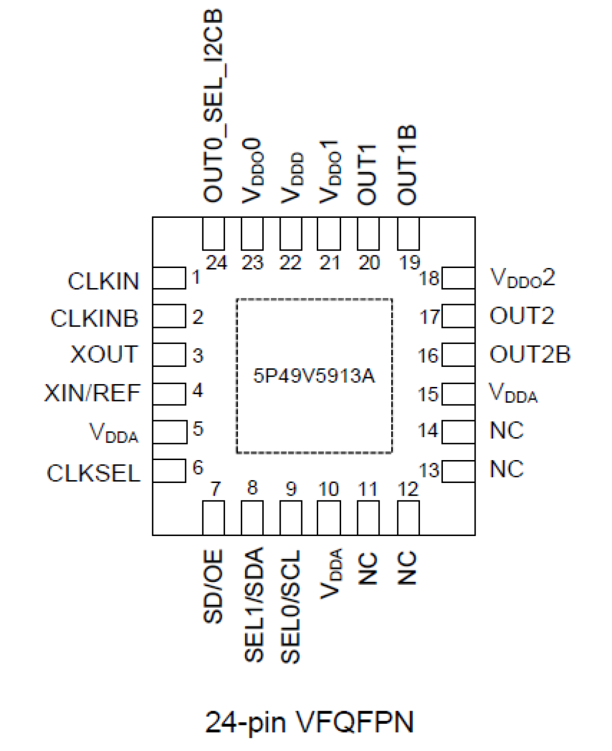
- 4x4 mm 24-ld VFQFPN
- -40° to +85°C operating temperature range
- Supported by Timing Commander™ software tool
描述
The 5P49V5913 is low-power programmable clock generator with best-in-class jitter performance and design flexibility with universal outputs capable of generating any output frequency. The 5P49V5913 is intended for high performance consumer, networking, industrial, computing, and data-communications applications. Configurations may be stored in on-chip One-Time Programmable (OTP) memory or changed using I2C interface. This is Renesas' fifth generation of programmable clock technology (VersaClock® 5). The frequencies are generated from a single reference clock or crystal input. A glitchless manual switchover function allows one of the redundant clock inputs to be selected during normal operation.
Two select pins allow up to 4 different configurations to be programmed and accessible using processor GPIOs or bootstrapping. The different selections may be used for different operating modes (full function, partial function, partial power-down), regional standards (US, Japan, Europe) or system production margin testing. The device may be configured to use one of two I2C addresses to allow multiple devices to be used in a system.
产品参数
| 属性 | 值 |
|---|---|
| App Jitter Compliance | PCIe Gen1, PCIe Gen2, PCIe Gen3 |
| Outputs (#) | 3 |
| Output Type | LVCMOS, LVPECL, HCSL, LVDS |
| Output Freq Range (MHz) | 1 - 350 |
| Input Freq (MHz) | 1 - 350 |
| Inputs (#) | 2 |
| Input Type | Crystal, LVCMOS, LVPECL, LVDS, HCSL |
| Output Banks (#) | 2 |
| Core Voltage (V) | 1.8V, 2.5V, 3.3V |
| Output Voltage (V) | 1.8V, 2.5V, 3.3V |
| Phase Jitter Typ RMS (ps) | 0.7 |
| Prog. Interface | I2C, OTP |
| Spread Spectrum | Yes |
封装选项
| Pkg. Type | Pkg. Dimensions (mm) | Lead Count (#) | Pitch (mm) |
|---|---|---|---|
| VFQFPN | 4.0 x 4.0 x 0.9 | 24 | 0.5 |
当前筛选条件
筛选
软件与工具
样例程序
模拟模型
Lab demonstration and clock jitter measurement showing VersaClock 5. The frequency analyzer shows phase jitter at approximately 575 picoseconds RMS. Presented by Baljit Chandhoke, product manager at IDT. For more information visit the Programmable Clocks page.
This video will show you how to program VersaClock® 5 Low Power Programmable Clock Generator.
Description
IDT's innovative support tool, Timing Commander™, expedites development cycles by empowering customers to program sophisticated timing devices with an intuitive and flexible Graphical User Interface. IDT's Timing Commander is a Windows™-based platform designed to serve user-friendly configuration interfaces, known as personalities, for various IDT products and product families. With a few simple clicks, the user is presented with a comprehensive, interactive block diagram offering the ability to modify desired input values, output values, and other configuration settings. The software automatically makes calculations, reports status monitors, and prepares register settings without the need to reference a datasheet. The tool also automatically loads the configuration settings over USB to an IDT evaluation board for immediate application in the circuit. Once the device has been configured and tuned for optimal system performance, the configuration file can be saved for factory-level programming before shipment. For more information about Timing Commander, visit our Timing Commander page.


