封装信息
| CAD 模型: | View CAD Model |
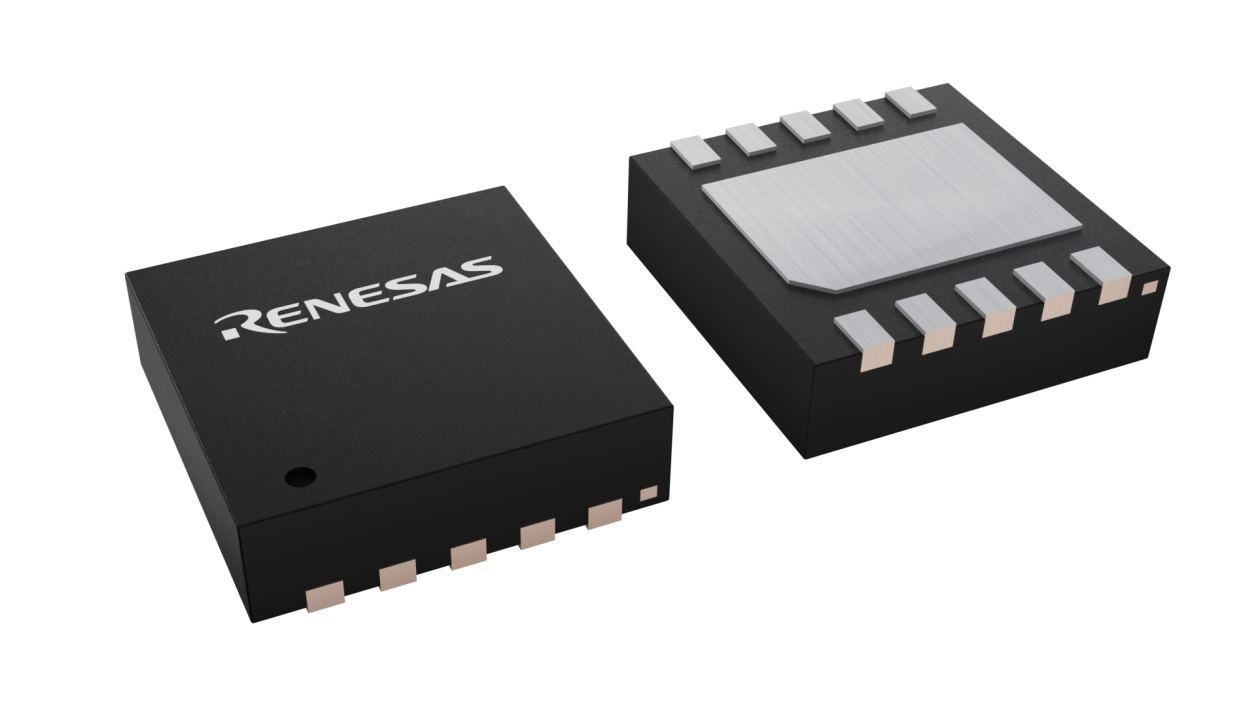
| Pkg. Type: | DFN |
| Pkg. Code: | LBR |
| Lead Count (#): | 10 |
| Pkg. Dimensions (mm): | 3.0 x 3.0 x 0.90 |
| Pitch (mm): | 0.5 |
环境和出口类别
| Moisture Sensitivity Level (MSL) | 3 |
| Pb (Lead) Free | Yes |
| ECCN (US) | EAR99 |
| HTS (US) | 8542.39.0090 |
| RoHS (ISL3259EIRZ-T) | 下载 |
产品属性
| Lead Count (#) | 10 |
| Carrier Type | Reel |
| Moisture Sensitivity Level (MSL) | 3 |
| Pitch (mm) | 0.5 |
| Pkg. Dimensions (mm) | 3.0 x 3.0 x 0.90 |
| Pb (Lead) Free | Yes |
| Pb Free Category | Pb-Free 100% Matte Tin Plate w/Anneal-e3 |
| Temp. Range (°C) | -40 to +85°C |
| Country of Assembly | MALAYSIA |
| Country of Wafer Fabrication | USA |
| Advanced Features | High Speed |
| Data Rate (Mbps) | 100 |
| Devices Allowed on Bus | 160 |
| Half/Full Duplex | Half |
| High ESD Protection | Yes-IEC61000 |
| Hot Plug | Yes |
| IS Enabled/Disabled | 2600/2600 µA |
| Length (mm) | 3 |
| MOQ | 6000 |
| Pkg. Type | DFN |
| Primary Feature | ESD Protected RS-485/422 |
| Qualification Level | Standard |
| Receivers (#) | 1 |
| SHDN ICC | <1 μA |
| Secondary Feature | High Speed |
| Slew Rate Limited | No |
| Supply Voltage Vcc (Min) (V) | 4.5 |
| Supply Voltage Vcc Range | 4.5-5.5 |
| Thickness (mm) | 0.9 |
| Transmitters (#) | 1 |
| Tx/Rx Enable | Yes |
| VL Pin | No |
| Width (mm) | 3 |
有关 ISL3259E 的资源
描述
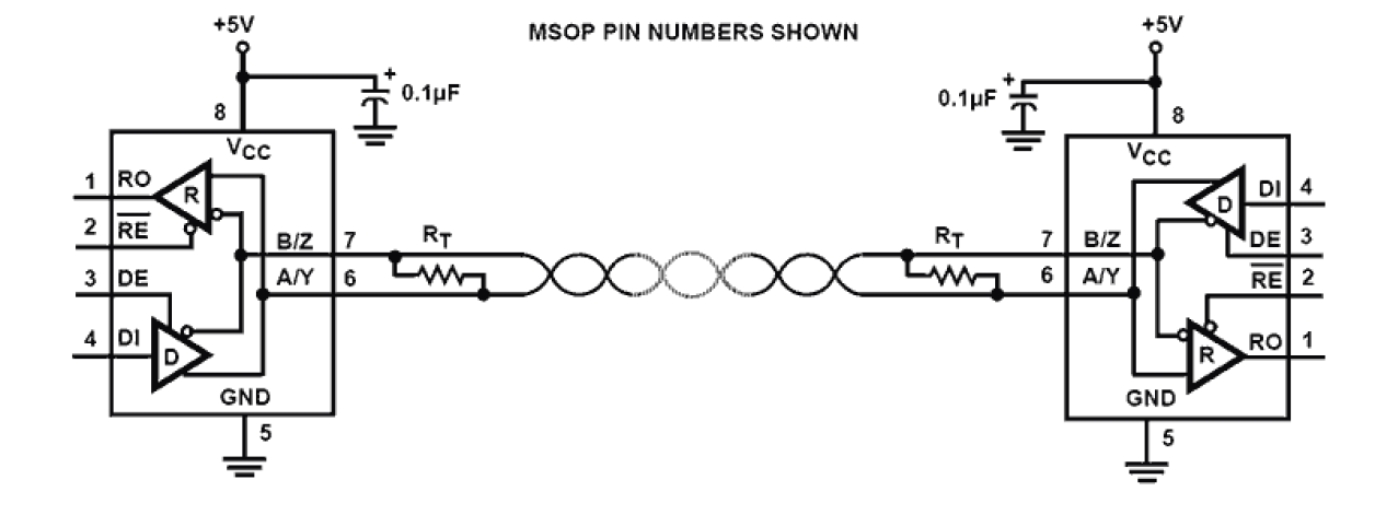
The ISL3259E is a ±15kV IEC 61000 ESD Protected, 5V powered, single transceiver that meets both the RS-485 and RS-422 standards for balanced communication. It also features the larger output voltage and higher data rate (up to 100Mbps) required by high-speed PROFIBUS applications. The low bus currents (+220μA/-150μA) present a 1/5 unit load to the RS-485 bus. This allows up to 160 transceivers on the network without violating the RS-485 specification’s load limit, and without using repeaters. This transceiver requires a 5V supply, and delivers at least a 2.1V differential output voltage. This translates into better noise immunity (data integrity), longer reach, or the ability to drive up to six 120Ω terminations in “star” or other non-standard bus topologies. SCSI applications benefit from the ISL3259E’s low receiver and transmitter part-to-part skews. The ISL3259E is perfect for high-speed parallel applications requiring simultaneous capture of large numbers of bits. The low bit-to-bit skew eases the timing constraints on the data latching signal. Receiver (Rx) inputs feature a “Full Fail-Safe” design, which ensures a logic high Rx output if Rx inputs are floating, shorted, or terminated but undriven. Rx outputs feature high drive levels (typically >30mA at VOL = 1V) to ease the design of optically isolated interfaces. Hot plug circuitry ensures that the Tx and Rx outputs remain in a high impedance state while the power supply stabilizes. Driver (Tx) outputs are short-circuit protected, even for voltages exceeding the power supply voltage. Additionally, on-chip thermal shutdown circuitry disables the Tx outputs to prevent damage if power dissipation becomes excessive.

