封装信息
| CAD 模型: | View CAD Model |
| Pkg. Type: | TQFN |
| Pkg. Code: | LKK |
| Lead Count (#): | 16 |
| Pkg. Dimensions (mm): | 3.0 x 3.0 x 0.75 |
| Pitch (mm): | 0.5 |
环境和出口类别
| Moisture Sensitivity Level (MSL) | |
| Pb (Lead) Free | No |
| ECCN (US) | EAR99 |
| HTS (US) | 8542.33.0001 |
| RoHS (ISL55211IRTZ-T7) | 下载 |
产品属性
| Lead Count (#) | 16 |
| Carrier Type | Reel |
| Pb (Lead) Free | No |
| Temp. Range (°C) | -40 to +85°C |
| 2nd Harmonic (dB) | -110 |
| 3rd Harmonic (dB) | -120 |
| Bandwidth (MHz) | 1400 |
| CMRR (dB) | 75 |
| Channels (#) | 1 |
| Enable | Yes |
| Gain Error / Measurement Error (Max) | 0.02 |
| Gain Min | 2 |
| IBIAS (nA) | 50000 |
| IOUT (A) | 0.045 |
| IS per Amp (mA) | 35 |
| Length (mm) | 3 |
| MOQ | 1000 |
| Noise VN (nV/√Hz) | 12 |
| Offset Voltage (Max) (mV) | 1.4 |
| PSRR (db) | 67 |
| Pitch (mm) | 0.5 |
| Pkg. Dimensions (mm) | 3.0 x 3.0 x 0.75 |
| Pkg. Type | TQFN |
| Qualification Level | Standard |
| Rail-to-Rail Input | No |
| Rail-to-Rail Output | No |
| Single Supply Voltage Range (V) | 3.3 - 4.2 |
| Slew Rate (V/µs) | 5600 |
| Thermal Shutdown | No |
| Thickness (mm) | 0.75 |
| Topology [Rail 1] | FDA |
| VOUT (V) | 2.35 |
| VS (Max) (V) | 4.2 |
| VS (Min) (V) | 3.3 |
| Width (mm) | 3 |
| field__slew_rate_typical_ | 5600 |
有关 ISL55211 的资源
描述
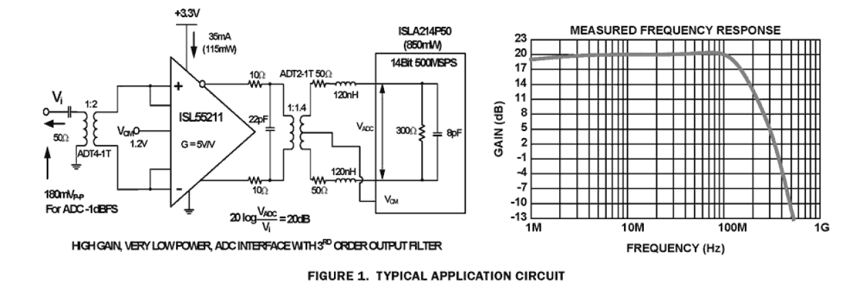
The ISL55211 is a wideband, differential input to differential output amplifier offering 3 possible internal gain settings. Using fixed 500Ω internal feedback resistors, the amplifier may be configured for a differential gain of 2, 4 or 5V/V depending on which combination of input pins are connected to the signal source. Internal feedback capacitors controls the signal bandwidth to be a constant 1. 4GHz in all gain settings. Ideally suited for AC-coupled data acquisition applications, the output DC common mode voltage is controlled through an external VCM pin or left to default to 1. 2V above the negative supply pin. Where the differential signal source is AC-coupled, the input common mode voltage will equal the output common mode voltage. Intended for very high dynamic range ADC interface applications, the ISL55211 offers 5600V/µs differential slew rate, 12nV/√Hz output noise, and >100dBc SFDR to >100MHz for 2VP-P 2-tone 3rd order intermodulation. Its balanced architecture effectively suppresses even order distortion terms - an important issue for very wide band 1st Nyquist zone ADC interface applications. Minimum gain operation of 2V/V (6dB) with 1dB peaking ensures stable performance over-temperature. It's ultra high differential slew rate of 5600V/µs provides adequate performance margin for large signal application through 500MHz. The ISL55211 requires only a single 3. 3V (max. 4. 2V) power supply and 35mA quiescent current, providing a very low power solution (115mW). Further power savings are possible using the optional power shutdown control - where the quiescent current can be reduced to 0. 4mA. A companion device, the ISL55210, offers similar performance where the feedback and gain resistors are external. Both are available in a 16 Ld TQFN (Pb-free) package and are specified for operation over the -40°C to +85°C ambient temperature range.
