封装信息
| CAD 模型: | View CAD Model |
| Pkg. Type: | QFN |
| Pkg. Code: | LJZ |
| Lead Count (#): | 28 |
| Pkg. Dimensions (mm): | 6.0 x 6.0 x 0.90 |
| Pitch (mm): | 0.7 |
环境和出口类别
| Moisture Sensitivity Level (MSL) | |
| Pb (Lead) Free | No |
| ECCN (US) | |
| HTS (US) |
产品属性
| Pkg. Type | QFN |
| Carrier Type | Tube |
| Lead Count (#) | 28 |
| Length (mm) | 6 |
| MOQ | 500 |
| Pb (Lead) Free | No |
| Pitch (mm) | 0.7 |
| Pkg. Dimensions (mm) | 6.0 x 6.0 x 0.90 |
| Qualification Level | Standard |
| Temp. Range (°C) | 0 to +70°C |
| Thickness (mm) | 0.9 |
| Width (mm) | 6 |
有关 ISL6532C 的资源
描述
Support is limited to customers who have already adopted these products.
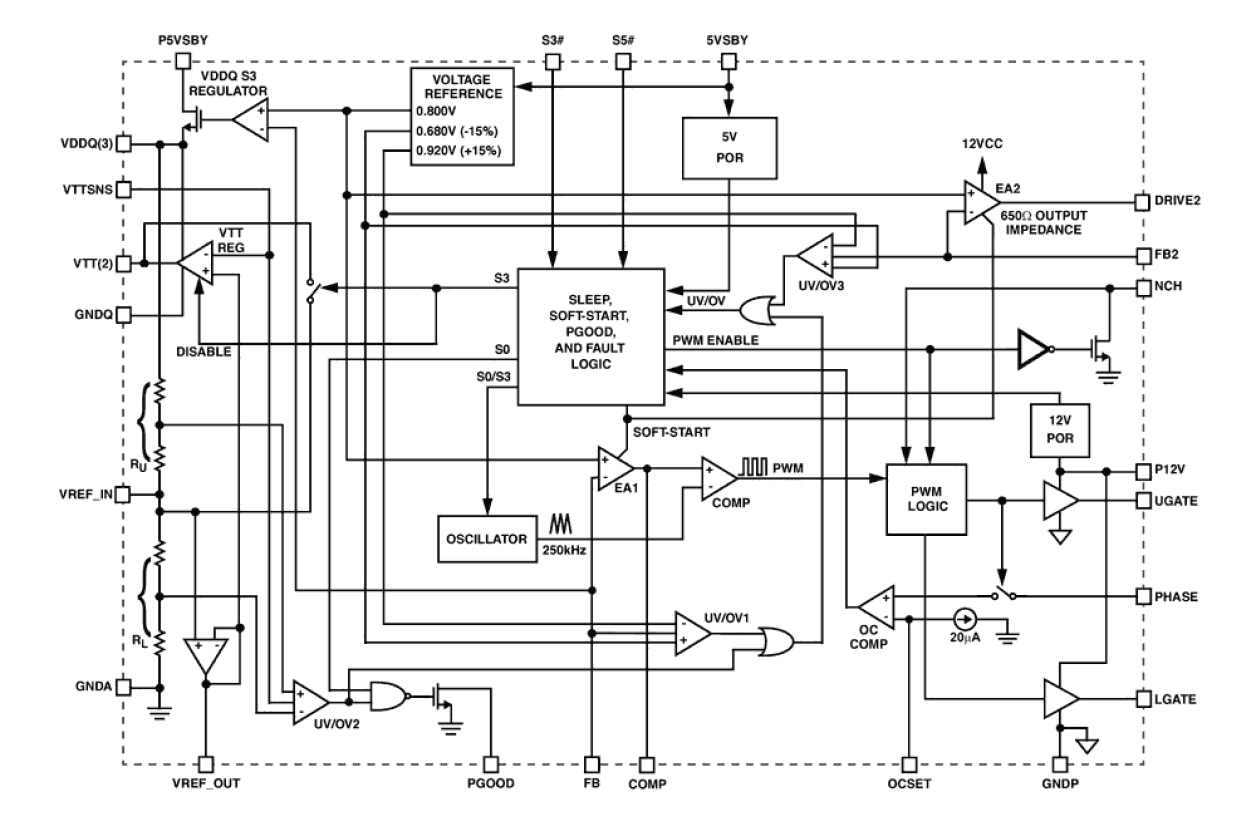
The ISL6532C provides a complete ACPI compliant power solution for up to 4 DIMM dual channel DDR/DDR2 Memory systems. Included are both a synchronous buck controller and integrated LDO to supply VDDQ with high current during S0/S1 states and standby current during S3 state. During S0/S1 state, a fully integrated sink-source regulator generates an accurate (VDDQ/2) high current VTT voltage without the need for a negative supply. A buffered version of the VDDQ/2 reference is provided as VREF. An LDO controller is also integrated for AGP core voltage regulation. The switching PWM controller drives two N-Channel MOSFETs in a synchronous-rectified buck converter topology. The synchronous buck converter uses voltage-mode control with fast transient response. Both the switching regulator and standby LDO provide a maximum static regulation tolerance of ±2% over line, load, and temperature ranges. The output is user-adjustable by means of external resistors down to 0. 8V. Switching memory core output between the PWM regulator and the standby LDO during state transitions is accomplished smoothly via the internal ACPI control circuitry. The NCH signal provides synchronized switching of a backfeed blocking switch during the transitions eliminating the need to route 5V Dual to the memory supply. An integrated soft-start feature brings all outputs into regulation in a controlled manner when returning to S0/S1 state from any sleep state. During S0 the PGOOD signal indicates VTT is within spec and operational. Each output is monitored for under and over-voltage events. The switching regulator has over current protection. Thermal shutdown is integrated.
