封装信息
| CAD 模型: | View CAD Model |
| Pkg. Type: | SOICW |
| Pkg. Code: | MWT |
| Lead Count (#): | 20 |
| Pkg. Dimensions (mm): | 12.9 x 7.5 x 0.00 |
| Pitch (mm): | 1.3 |
环境和出口类别
| Moisture Sensitivity Level (MSL) | 3 |
| Pb (Lead) Free | Yes |
| RoHS (ISL81387IBZ) | 下载 |
| ECCN (US) | |
| HTS (US) |
产品属性
| Lead Count (#) | 20 |
| Carrier Type | Tube |
| Moisture Sensitivity Level (MSL) | 3 |
| Pitch (mm) | 1.3 |
| Pkg. Dimensions (mm) | 12.9 x 7.5 x 0.00 |
| Pb (Lead) Free | Yes |
| Pb Free Category | Pb-Free 100% Matte Tin Plate w/Anneal-e3 |
| Temp. Range (°C) | -40 to +85°C |
| Data Rate RS-485/RS-232 | 20, 0.46, 0.115 /0.65 |
| High ESD (kV) | 15 |
| Length (mm) | 12.9 |
| Loopback Feature | Yes |
| MOQ | 760 |
| Operating Supply Current Icc RS-485/RS-232 | 1.6/3.7 |
| Pkg. Type | SOICW |
| Ports (#) | 1 |
| Price (USD) | $5.16614 |
| Qualification Level | Standard |
| RS-485 Rx Failsafe Type | Full |
| RXEN Polarity | High |
| SHDN ICC | 35 µA |
| Supported Protocols | RS-232, RS-422, RS-485 |
| Tx/Rx per Port (#) | 1 |
| VCC (V) | 5 |
| VLOGIC Supply Pin? | No |
| Width (mm) | 7.5 |
有关 ISL81387 的资源
描述
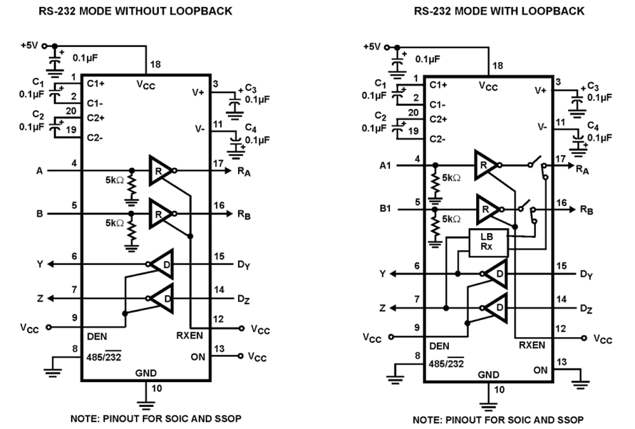
These devices are BiCMOS interface ICs that are user configured as either a single RS-422, RS-485 differential transceiver, or as a dual (2 Tx, 2 Rx) RS-232 transceiver. In RS-232 mode, the on-board charge pump generates RS-232 compliant ±5V Tx output levels, from a supply as low as 4.5V. Four small 0.1µF capacitors are required for the charge pump. The transceivers are RS-232 compliant, with the Rx inputs handling up to ±25V, and the Tx outputs handling ±12V. In RS-485 mode, the transceivers support both the RS-485 and RS-422 differential communication standards. The RS-485 receiver features full fail-safe operation, so the Rx output remains in a high state if the inputs are open or shorted together. The RS-485 transmitter supports up to three data rates, two of which are slew rate limited for problem-free communications. The charge pump disables in RS-485 mode, thereby saving power, minimizing noise and eliminating the charge pump capacitors. Both RS-232, RS-485 modes feature loopback and shutdown functions. The loopback mode internally connects the Tx outputs to the corresponding Rx input, which facilitates the implementation of board level self-test functions. The outputs remain connected to the loads during loopback, so connection problems (e. g., shorted connectors or cables) can be detected. The shutdown mode disables the Tx and Rx outputs, disables the charge pump if in RS-232 mode, and places the IC in a low current (35µA) mode. The ISL41387 is a QFN packaged device that offers additional functionality, including a lower speed and edge rate option (115kbps) for EMI sensitive designs, or to allow longer bus lengths. It also features a logic supply voltage pin (VL) that sets the VOH level of logic outputs, and the switching points of logic inputs, to be compatible with another supply voltage in mixed voltage systems. The QFN's choice of active high or low Rx enable pins increases design flexibility, allowing Tx/Rx direction control via a single signal by connecting DEN and RXEN together. For a dual port version of these devices, please see the ISL81334, ISL41334 datasheet.

