封装信息
| CAD 模型: | View CAD Model |
| Pkg. Type: | SOIC |
| Pkg. Code: | MOQ |
| Lead Count (#): | 8 |
| Pkg. Dimensions (mm): | 4.9 x 3.9 x 1.5 |
| Pitch (mm): | 1.27 |
环境和出口类别
| Moisture Sensitivity Level (MSL) | 3 |
| Pb (Lead) Free | Yes |
| RoHS (ISL8483EIBZ) | 下载 |
| ECCN (US) | |
| HTS (US) |
产品属性
| Lead Count (#) | 8 |
| Carrier Type | Tube |
| Moisture Sensitivity Level (MSL) | 3 |
| Pb (Lead) Free | Yes |
| Pb Free Category | Pb-Free 100% Matte Tin Plate w/Anneal-e3 |
| Temp. Range (°C) | -40 to +85°C |
| Country of Assembly | TAIWAN |
| Country of Wafer Fabrication | UNITED STATES |
| Advanced Features | Low Cost |
| Data Rate (Mbps) | 0.25 |
| Devices Allowed on Bus | 32 |
| Half/Full Duplex | Half |
| High ESD Protection | Yes |
| Hot Plug | No |
| IS Enabled/Disabled | 470/160 µA |
| Length (mm) | 4.9 |
| MOQ | 3920 |
| Pitch (mm) | 1.3 |
| Pkg. Dimensions (mm) | 4.9 x 3.9 x 0.00 |
| Pkg. Type | SOICN |
| Price (USD) | $0.72742 |
| Primary Feature | Standard RS-485/422 |
| Qualification Level | Standard |
| Receivers (#) | 1 |
| SHDN ICC | 0.001 µA |
| Slew Rate Limited | Yes |
| Supply Voltage Vcc (Min) (V) | 4.5 |
| Supply Voltage Vcc Range | 4.5-5.5 |
| Transmitters (#) | 1 |
| Tx/Rx Enable | Yes |
| VL Pin | No |
| Width (mm) | 3.9 |
有关 ISL8483E 的资源
描述
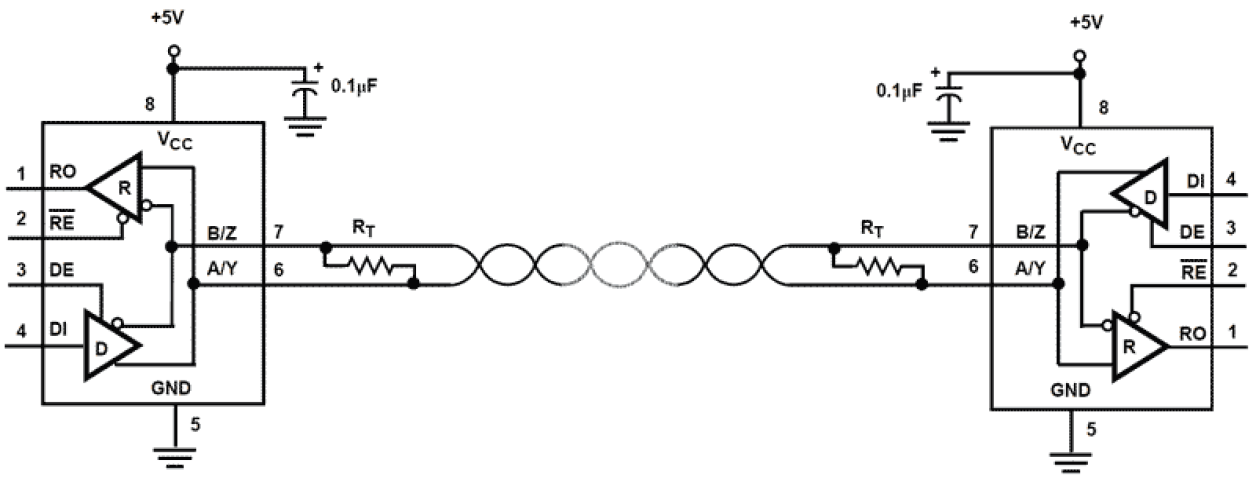
The ISL8483E and ISL8485E are ESD protected, BiCMOS 5V powered, single transceivers that meet both the RS-485 and RS-422 standards for balanced communication. Each driver output/receiver input is protected against ±15kV ESD strikes without latch-up. Unlike competitive devices, this Renesas family is specified for 10% tolerance supplies (4. 5V to 5. 5V). The ISL8483E uses slew rate limited drivers that reduce EMI and minimize reflections from improperly terminated transmission lines or unterminated stubs in multidrop and multipoint applications. Data rates up to 10Mbps are achievable by using the ISL8485E, which features higher slew rates. Both devices present a “single unit load” to the RS-485 bus, which allows up to 32 transceivers on the network. Receiver (Rx) inputs feature a “fail-safe if open” design, which ensures a logic high Rx output if Rx inputs are floating. Driver (Tx) outputs are short-circuit protected even for voltages exceeding the power supply voltage. Additionally, on-chip thermal shutdown circuitry disables the Tx outputs to prevent damage if power dissipation becomes excessive. These half duplex configurations multiplex the Rx inputs and Tx outputs to allow transceivers with Rx and Tx disable functions in 8 Ld packages.
