封装信息
| CAD 模型: | View CAD Model |
| Pkg. Type: | WLCSP-4 |
| Pkg. Code: | |
| Lead Count (#): | 4 |
| Pkg. Dimensions (mm): | 0.8 x 0.8 mm |
| Pitch (mm): |
环境和出口类别
| ECCN (US) | EAR99 |
| HTS (US) | 8542.39.0090 |
| Pb (Lead) Free | |
| Moisture Sensitivity Level (MSL) |
产品属性
| Lead Count (#) | 4 |
| Temp. Range (°C) | -40 to +85°C |
| Current Monitor Output | No |
| Discharge Circuit | Yes |
| Enable | Active High |
| FET Pass Device Type | Single P-Channel |
| IDS (A) | 2.2 |
| IDS Channel 1 (A) | 2.2 |
| Internal TVS Surge Protection | No |
| Output Discharge Circuit | Yes |
| Output Voltage Slew Rate set by | No |
| Over Current Protection (OCP) | Fixed Inrush Current Limit |
| Over Current Protection Setting Range Channel 1 | 0.0165 - 0.0165 |
| Over Temperature Protection (OTP) | No |
| Over Voltage Protection | No |
| Over Сurrent Protection Setting Range (A) | 0.0165 - 0.0165 |
| Parametric Category | Load Switches |
| Pkg. Dimensions (mm) | 0.8 x 0.8 mm |
| Pkg. Type | WLCSP-4 |
| Power Good (PG), FAULT indicator | No |
| Power Monitor Output | No |
| Protection Features | Fixed IIN |
| RDSON (Typ) (mΩ) | 33 |
| RDSON (Typ) Channel 1 (mΩ) | 33 |
| Ramp Control | No |
| Reverse current blocking | No |
| Reverse voltage detection | No |
| Short Circuit Protection | No |
| Undervoltage Protection | No |
| VD/VIN (Max) | 5.5 |
| VD/VIN (Min) | 2.5 |
| VIN Channel 1 max. (V) | 5.5 |
| VIN Channel 1 min. (V) | 2.5 |
| VIN Range (V) | 2.5 - 5.5 |
| VIN Range Channel 1 (V) | 2.5 - 5.5 |
| VIN max. (V) | V5.5 |
| VIN min. (V) | V2.5 |
| VOUT Discharge Circuit | Yes |
有关 SLG59M1736C 的资源
描述
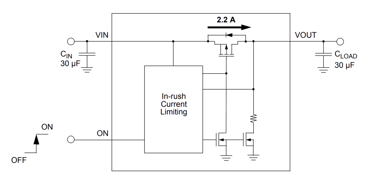
Operating from a 2.5V to 5.5V power supply, the SLG59M1736C is a self‑powered, high‑performance 33mΩ, 2.2A single-channel pFET load switch with a controlled VIN inrush current profile. The SLG59M1736C’s low supply current and controlled VIN inrush current profile make it an ideal pFET load switch in small form factor personal health monitor and watch applications. Using a proprietary MOSFET design, the SLG59M1736C achieves a low RDSON across the entire input voltage range. Through the application of proprietary technology, the SLG59M1736C’s can be used in applications up to 2.2A with a very‑small 0.64mm² WLCSP form factor.
