特性
- < 100mW 核心功率(3.3V 电压)
- < 0.5ps RMS 相位抖动(典型值)
- PCIe Gen 1/2/3/4/5 扩频关闭
- PCIe Gen 1/2/3/4 扩频开启
- 1/10GbE,USB 3.0 接口
- 支持晶振(8MHz–40MHz)和外部时钟输入(1MHz–350MHz)
- 4 个通用输出对:LVPECL、LVDS、HCSL 或 8 个 LVCMOS 输出
- 4 个独立频率,输出范围为 0.001MHz–350MHz
- 参考输出
- 1.8V / 2.5V / 3.3V 核心和输出电压
- 2 个可编程的 I²C 地址允许多个设备在同一系统中运行。
- OTP 非易失内存性存储器中可储存最多 4 种不同的配置集
- 由 Renesas IC Toolbox (RICBox) 软件工具提供支持
- 具有线上表单提交功能,支持快速采样和定制流程
- 4 x 4 mm 24-VFQFPN 封装
- 工作温度范围:-40°C 至 +85°C


描述
产品参数
| 属性 | 值 |
|---|---|
| Diff. Outputs | 4 |
| App Jitter Compliance | PCIe Gen1, PCIe Gen2, PCIe Gen3, PCIe Gen4, PCIe Gen5 |
| Outputs (#) | 5 |
| Output Type | LVCMOS, LVPECL, HCSL, LVDS |
| Output Freq Range (MHz) | 1 - 350 |
| Input Freq (MHz) | 1 - 350 |
| Inputs (#) | 2 |
| Input Type | Crystal, LVCMOS, LVPECL, LVDS, HCSL |
| Output Banks (#) | 4 |
| Core Voltage (V) | 1.8V, 2.5V, 3.3V |
| Output Voltage (V) | 1.8V, 2.5V, 3.3V |
| Product Category | VersaClock 6E, Low Jitter Clocks (<700 fs RMS), General Purpose Clocks, PCI Express Clocks, Programmable Clocks |
| Selection Criteria | <700 fs RM |
封装选项
| Pkg. Type | Pkg. Dimensions (mm) | Lead Count (#) | Pitch (mm) |
|---|---|---|---|
| VFQFPN | 4.0 x 4.0 x 0.9 | 24 | 0.5 |
产品对比
应用方框图
 | 视觉 AI 盒 作为集中控制枢纽,用于管理多路摄像头和 AI 模型。 |
 | 多显示器 HMI SoM 具有优化功耗和时序的 SOM 支持多显示器嵌入式应用。 |
 | 支持 4K 视频的全功能 HMI 高性能 HMI 设计提供无缝丝滑的 4K 视频、高级图形和可靠的连接。 |
完成您的设计
寻找相关的产品,完善您的设计
Renesas Boards & Kits
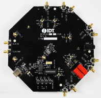
Evaluation Board for 5P49V6965 VersaClock 6E
This is the evaluation board for the 5P49V6965 VersaClock® 6E programmable clock generator. With RMS phase jitter of less than 0.5ps over the full 12kHz to 20MHz integration range, the device meets the stringent jitter requirements of PCI Express® Gen 1/2/3, USB 3.0, and 1G/10G Ethernet.
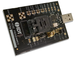
Programming Kit for VersaClock 6E
The VersaClock® 6E programmer board is made to ease the programming of 5P49V6965 and 5P49V6975 blank devices. With the onboard USB interface, Renesas IC Toolbox's (RICBox) graphical user interface (GUI) can be used to communicate with the blank device in the socket for configuration and... 阅读详情
Partner Boards & Kits
RZ/G2 Series System on Module (SoM)
NEW支持社区
-
5p49v6965输出频率异常
您好,我在使用5p49v6965过程中,配置了相应的输出频率,使用示波器测量,每个频率都比计算值大8%左右。读出寄存器值对比RICBox以 ...
2026年4月20日 -
5P49V6965软件配置后时钟没有输出或者没稳定
您好, 之前安装官方的软件做配置,配置有效,但是实际发现配置完成后时钟还没出或者没有稳定,请问配置完成后需要等 ...
2026年4月29日 -
5P49V6965使用问题
麻烦问一下,5P49V6965芯片使用问题,手册中写到如果使用硬件配置,SEL0和SEL1配置的4种CFG0~3,对应输出的时钟是多少Mhz,输入时钟 ...
2024年5月31日


