封装信息
| CAD 模型: | View CAD Model |
| Pkg. Type: | QSOP |
| Pkg. Code: | PCG20 |
| Lead Count (#): | 20 |
| Pkg. Dimensions (mm): | 8.7 x 3.8 x 1.47 |
| Pitch (mm): | 0.64 |
环境和出口类别
| Moisture Sensitivity Level (MSL) | 1 |
| Pb (Lead) Free | Yes |
| ECCN (US) | EAR99 |
| HTS (US) | 8542.39.0090 |
产品属性
| Lead Count (#) | 20 |
| Carrier Type | Tube |
| Moisture Sensitivity Level (MSL) | 1 |
| Qty. per Reel (#) | 0 |
| Qty. per Carrier (#) | 55 |
| Package Area (mm²) | 33.1 |
| Pitch (mm) | 0.64 |
| Pkg. Dimensions (mm) | 8.7 x 3.8 x 1.47 |
| Pb (Lead) Free | Yes |
| Pb Free Category | e3 Sn |
| Temp. Range (°C) | -40 to 85°C |
| Country of Assembly | TAIWAN |
| Country of Wafer Fabrication | TAIWAN, USA |
| Core Voltage (V) | 3.3 |
| Function | Buffer |
| Input Type | LVCMOS |
| Inputs (#) | 2 |
| Length (mm) | 8.7 |
| MOQ | 495 |
| Output Banks (#) | 2 |
| Output Skew (ps) | 500 |
| Output Type | LVCMOS |
| Output Voltage (V) | 3.3 |
| Outputs (#) | 10 |
| Pkg. Type | QSOP |
| Price (USD) | $0.96329 |
| Product Category | Clock Buffers & Drivers |
| Requires Terms and Conditions | Does not require acceptance of Terms and Conditions |
| Tape & Reel | No |
| Thickness (mm) | 1.47 |
| Width (mm) | 3.8 |
| 已发布 | No |
有关 49FCT3805 的资源
描述
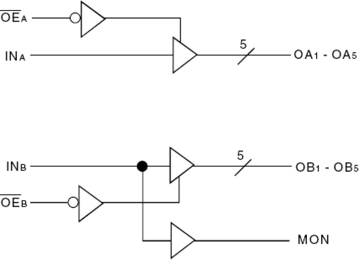
The FCT3805 is a 3.3 volt, non-inverting clock driver built using advanced dual metal CMOS technology. The device consists of two banks of drivers, each with a 1:5 fanout and its own output enable control. The device has a "heartbeat" monitor for diagnostics and PLL driving. The MON output is identical to all other outputs and complies with the output specifications in this document. The FCT3805 offers low capacitance inputs with hysteresis. The FCT3805 is designed for high speed clock distribution where signal quality and skew are critical. The FCT3805 also allows single point-to-point transmission line driving in applications such as address distribution, where one signal must be distributed to multiple receivers with low skew and high signal quality. For more information on using the FCT3805 with two different input frequencies on bank A and B, please see AN-236.
