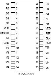
封装信息
| CAD 模型: | View CAD Model |
| Pkg. Type: | QSOP |
| Pkg. Code: | PCG28 |
| Lead Count (#): | 28 |
| Pkg. Dimensions (mm): | 9.9 x 3.8 x 1.47 |
| Pitch (mm): | 0.64 |
环境和出口类别
| Moisture Sensitivity Level (MSL) | 1 |
| Pb (Lead) Free | Yes |
| ECCN (US) | EAR99 |
| HTS (US) | 8542.39.0090 |
产品属性
| Lead Count (#) | 28 |
| Carrier Type | Tube |
| Moisture Sensitivity Level (MSL) | 1 |
| Output Freq Range (MHz) | 1.2 - 160 |
| Qty. per Reel (#) | 0 |
| Qty. per Carrier (#) | 48 |
| Pb (Lead) Free | Yes |
| Pb Free Category | e3 Sn |
| Temp. Range (°C) | 0 to 70°C |
| Advanced Features | Reference Output |
| Core Voltage (V) | 3.3V, 5V |
| Feedback Input | No |
| Input Freq (MHz) | 2 - 50 |
| Input Type | Crystal, LVCMOS |
| Inputs (#) | 1 |
| Length (mm) | 9.9 |
| MOQ | 2544 |
| Output Banks (#) | 2 |
| Output Type | LVCMOS |
| Output Voltage (V) | 3.3V, 5V |
| Outputs (#) | 2 |
| Package Area (mm²) | 37.6 |
| Period Jitter Typ P-P (ps) | 140 |
| Pitch (mm) | 0.64 |
| Pkg. Dimensions (mm) | 9.9 x 3.8 x 1.47 |
| Pkg. Type | QSOP |
| Prog. Clock | No |
| Reference Output | Yes |
| Requires Terms and Conditions | Does not require acceptance of Terms and Conditions |
| Spread Spectrum | No |
| Tape & Reel | No |
| Thickness (mm) | 1.47 |
| Width (mm) | 3.8 |
| 已发布 | No |
有关 525-01 的资源
描述
The 525-01/02 are the most flexible way to generate a high-quality, high-accuracy, high-frequency clock output from an inexpensive crystal or clock input. These devices are designed to replace crystal oscillators in almost any electronic system. The user can configure the device to produce nearly any output frequency from any input frequency by grounding or floating the select pins. Neither microcontroller, software, nor device programmer are needed to set the frequency. Using Phase-Locked Loop (PLL) techniques, the device accepts a standard fundamental mode, inexpensive crystal to produce output clocks up to 250 MHz. It can also produce a highly accurate output clock from a given input clock, keeping them frequency locked together. For similar capability with a serial interface, use the 307. For simple multipliers to produce common frequencies, refer to the PLL Clock Multiplier family of parts, which are smaller and more cost effective. This product is intended for clock generation. It has low output jitter (variation in the output period), but input to output skew and jitter are not defined nor guaranteed. For applications which require defined input to output timing, use the 527-01.

