封装信息
| CAD 模型: | View CAD Model |
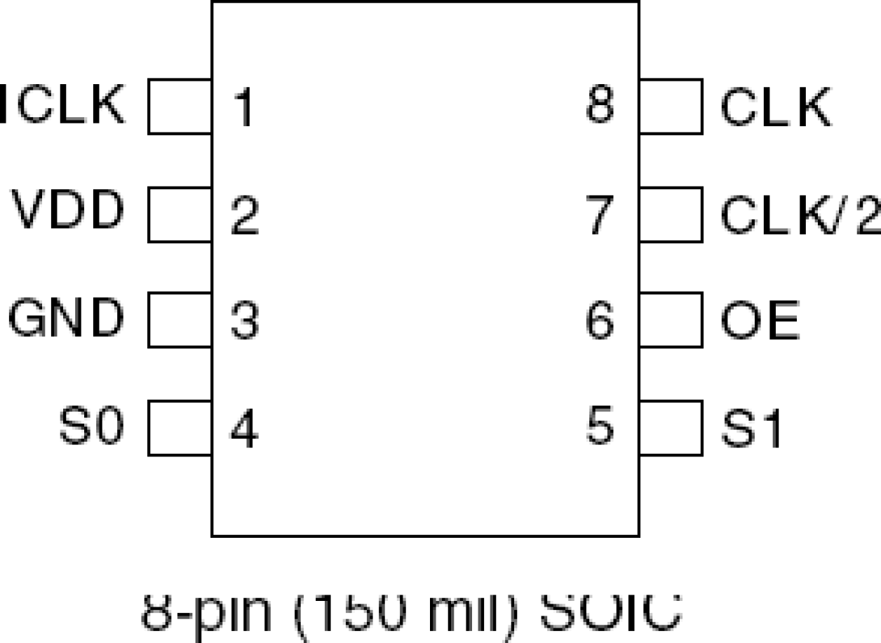
| Pkg. Type: | SOIC |
| Pkg. Code: | DCG8 |
| Lead Count (#): | 8 |
| Pkg. Dimensions (mm): | 4.9 x 3.9 x 1.5 |
| Pitch (mm): | 1.27 |
环境和出口类别
| Moisture Sensitivity Level (MSL) | 1 |
| Pb (Lead) Free | Yes |
| ECCN (US) | EAR99 |
| HTS (US) | 8542.39.0090 |
产品属性
| Lead Count (#) | 8 |
| Carrier Type | Reel |
| Moisture Sensitivity Level (MSL) | 1 |
| Qty. per Reel (#) | 3000 |
| Qty. per Carrier (#) | 0 |
| Pb (Lead) Free | Yes |
| Pb Free Category | e3 Sn |
| Temp. Range (°C) | 0 to 70°C |
| Core Voltage (V) | 3.3 |
| Divider Value | 2, 4, 6, 8, 12, 16 |
| Function | Buffer |
| Input Freq (MHz) | 156 |
| Input Type | LVCMOS |
| Inputs (#) | 1 |
| Length (mm) | 4.9 |
| MOQ | 3000 |
| Output Banks (#) | 2 |
| Output Freq Range (MHz) | 156 |
| Output Skew (ps) | 500 |
| Output Type | LVCMOS |
| Output Voltage (V) | 3.3 |
| Outputs (#) | 2 |
| Package Area (mm²) | 19.1 |
| Pitch (mm) | 1.27 |
| Pkg. Dimensions (mm) | 4.9 x 3.9 x 1.5 |
| Pkg. Type | SOIC |
| Price (USD) | $8.48802 |
| Product Category | Clock Buffers & Drivers |
| Reel Size (in) | 13 |
| Requires Terms and Conditions | Does not require acceptance of Terms and Conditions |
| Tape & Reel | Yes |
| Thickness (mm) | 1.5 |
| Width (mm) | 3.9 |
| 已发布 | No |
有关 542 的资源
描述
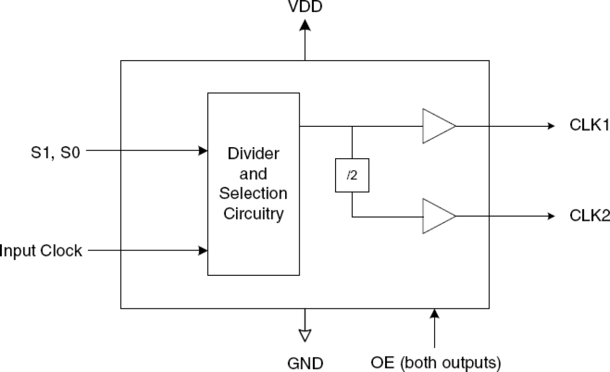
The 542 is cost effective way to produce a high-quality clock output divided from a clock input. The chip accepts a clock input up to 156 MHz at 3.3 V and produces a divide by 2, 4, 6, 8, 12, or 16 of the input clock. There are two outputs on the chip, one being a low-skew divide by two of the other. For instance, if an 100 MHz input clock is used, the 542 can produce low-skew 50 MHz and 25 MHz clocks, or low skew 25 MHz and 12.5 MHz clocks. The chip has an all-chip power-down mode that stops the outputs low, and an OE pin that tri-states the outputs. See the 501, 502, 511, 512, and 525 for clock multipliers.


