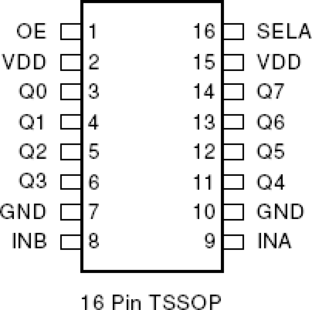
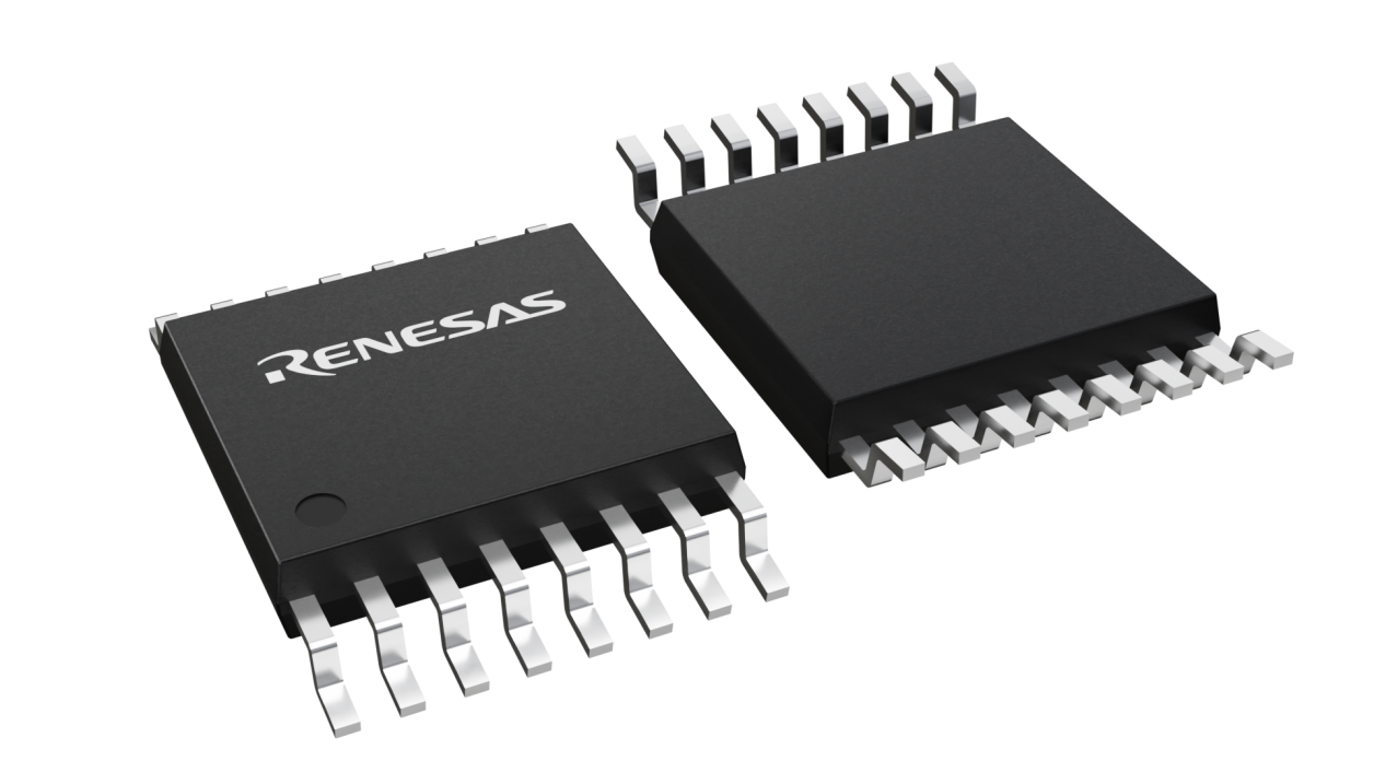
封装信息
| CAD 模型: | View CAD Model |
| Pkg. Type: | TSSOP |
| Pkg. Code: | PGG16 |
| Lead Count (#): | 16 |
| Pkg. Dimensions (mm): | 5.0 x 4.4 x 1.0 |
| Pitch (mm): | 0.65 |
环境和出口类别
| Moisture Sensitivity Level (MSL) | 1 |
| Pb (Lead) Free | Yes |
| ECCN (US) | EAR99 |
| HTS (US) | 8542.39.0090 |
产品属性
| Lead Count (#) | 16 |
| Carrier Type | Reel |
| Moisture Sensitivity Level (MSL) | 1 |
| Qty. per Reel (#) | 2500 |
| Qty. per Carrier (#) | 0 |
| Pb (Lead) Free | Yes |
| Pb Free Category | e3 Sn |
| Temp. Range (°C) | -40 to 85°C |
| Country of Assembly | TAIWAN |
| Country of Wafer Fabrication | TAIWAN |
| Core Voltage (V) | 2.5V, 3.3V, 5V |
| Function | Buffer, Multiplexer |
| Input Freq (MHz) | 200 |
| Input Type | LVCMOS |
| Inputs (#) | 2 |
| Length (mm) | 5 |
| MOQ | 2500 |
| Output Banks (#) | 1 |
| Output Freq Range (MHz) | 200 |
| Output Skew (ps) | 50 |
| Output Type | LVCMOS |
| Output Voltage (V) | 2.5V, 3.3V, 5V |
| Outputs (#) | 8 |
| Package Area (mm²) | 22 |
| Pitch (mm) | 0.65 |
| Pkg. Dimensions (mm) | 5.0 x 4.4 x 1.0 |
| Pkg. Type | TSSOP |
| Price (USD) | $3.62075 |
| Reel Size (in) | 13 |
| Requires Terms and Conditions | Does not require acceptance of Terms and Conditions |
| Tape & Reel | Yes |
| Thickness (mm) | 1 |
| Width (mm) | 4.4 |
| 已发布 | No |
有关 552-02 的资源
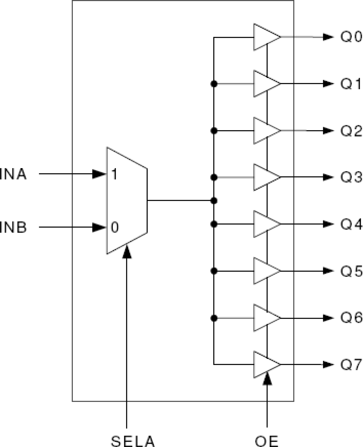
描述
The 552-02 is a low skew, single-input to eight-output clock buffer. The device offers a dual input with pin select for switching between two clock sources. It is part of Renesas' ClockBlocks™ family. See the 553 for a 1 to 4 low skew buffer. For more than 8 outputs see the MK74CBxxx Buffalo™ series of clock drivers. Renesas makes many non-PLL and PLL based low skew output devices as well as Zero Delay Buffers to synchronize clocks. Contact us for all of your clocking needs.


