封装信息
| CAD 模型: | View CAD Model |
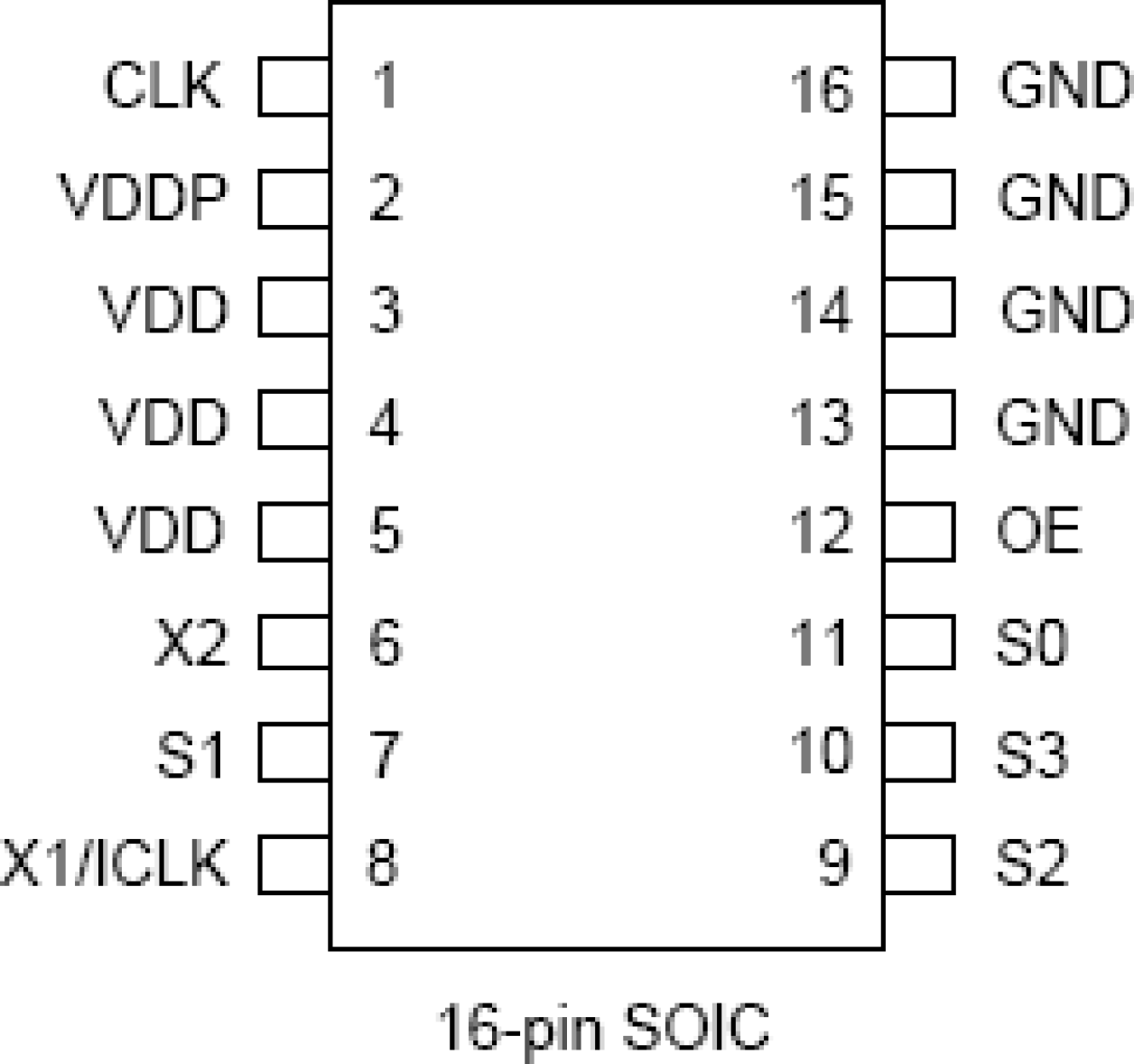
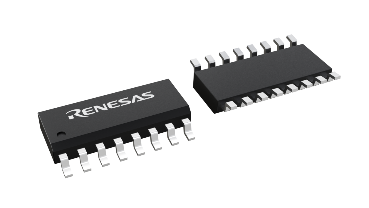
| Pkg. Type: | SOIC |
| Pkg. Code: | DCG16 |
| Lead Count (#): | 16 |
| Pkg. Dimensions (mm): | 9.9 x 3.9 x 1.5 |
| Pitch (mm): | 1.27 |
环境和出口类别
| Moisture Sensitivity Level (MSL) | 3 |
| Pb (Lead) Free | Yes |
| ECCN (US) | EAR99 |
| HTS (US) | 8542.39.0090 |
产品属性
| Lead Count (#) | 16 |
| Carrier Type | Tube |
| Moisture Sensitivity Level (MSL) | 3 |
| Qty. per Reel (#) | 0 |
| Qty. per Carrier (#) | 48 |
| Pb (Lead) Free | Yes |
| Pb Free Category | e3 Sn |
| Temp. Range (°C) | -40 to 85°C |
| C-C Jitter Max P-P (ps) | 18 |
| Core Voltage (V) | 3.3V, 5V |
| Feedback Input | No |
| Input Freq (MHz) | 10 - 27 |
| Input Type | Crystal, LVCMOS |
| Inputs (#) | 1 |
| Length (mm) | 9.9 |
| MOQ | 144 |
| Output Banks (#) | 1 |
| Output Freq Range (MHz) | 13.33 - 170 |
| Output Type | LVCMOS |
| Output Voltage (V) | 2.5V, 3.3V |
| Outputs (#) | 1 |
| Package Area (mm²) | 38.6 |
| Period Jitter Max P-P (ps) | 75 |
| Period Jitter Typ P-P (ps) | 50 |
| Pitch (mm) | 1.27 |
| Pkg. Dimensions (mm) | 9.9 x 3.9 x 1.5 |
| Pkg. Type | SOIC |
| Product Category | General Purpose Clocks |
| Prog. Clock | No |
| Reference Output | No |
| Requires Terms and Conditions | Does not require acceptance of Terms and Conditions |
| Spread Spectrum | No |
| Tape & Reel | No |
| Thickness (mm) | 1.5 |
| Width (mm) | 3.9 |
| 已发布 | No |
有关 601-02 的资源
描述
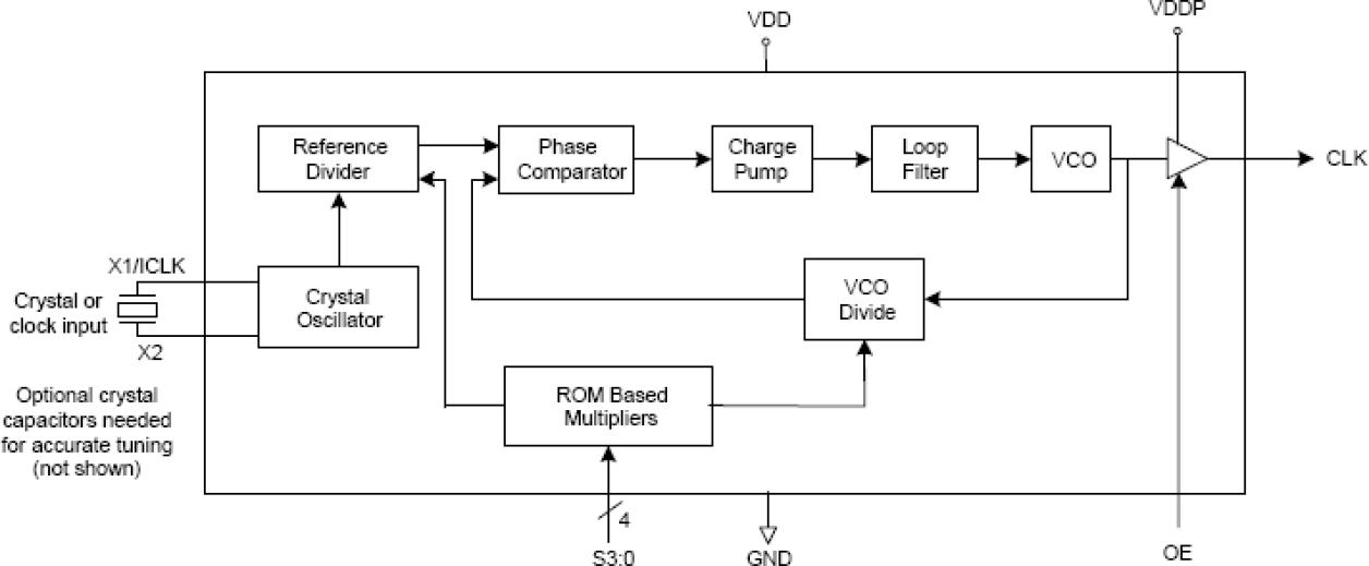
The 601-02 is a low cost, low phase noise, high performance clock synthesizer for any application that requires low phase noise and low jitter. The 601 is IDT's lowest phase noise multiplier. Using IDT's patented analog and digital Phase Locked Loop (PLL) techniques, the chip accepts a 10–27 MHz crystal or clock input, and produces output clocks up to 170 MHz at 3.3 V. A separate supply pin is provided so that the output can be 2.5 V. This product is intended for clock generation. It has low output jitter (variation in the output period), but input to output skew and jitter are not defined nor guaranteed. For applications which require defined input to output timing, use the 670-01.


