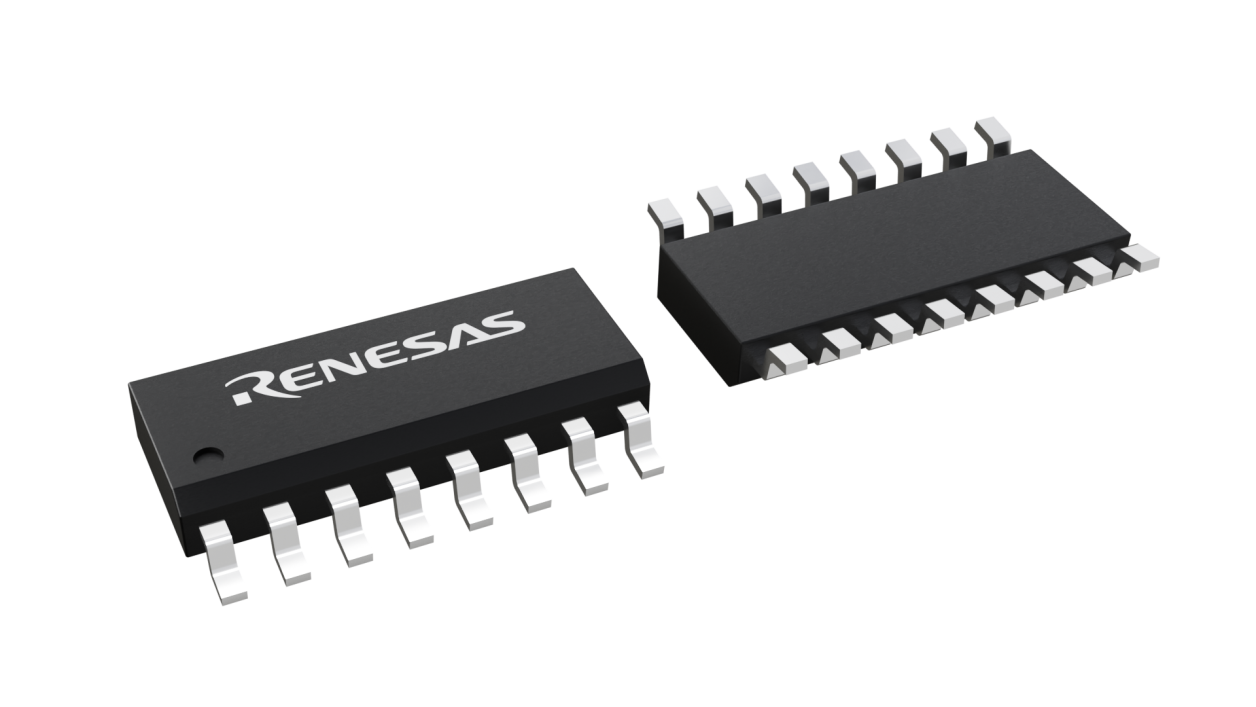
封装信息
| CAD 模型: | View CAD Model |
| Pkg. Type: | SOIC |
| Pkg. Code: | DCG16 |
| Lead Count (#): | 16 |
| Pkg. Dimensions (mm): | 9.9 x 3.9 x 1.5 |
| Pitch (mm): | 1.27 |
环境和出口类别
| Moisture Sensitivity Level (MSL) | 3 |
| Pb (Lead) Free | Yes |
| ECCN (US) | EAR99 |
| HTS (US) | 8542.39.0090 |
产品属性
| Lead Count (#) | 16 |
| Carrier Type | Tube |
| Moisture Sensitivity Level (MSL) | 3 |
| Qty. per Reel (#) | 0 |
| Qty. per Carrier (#) | 48 |
| Pb (Lead) Free | Yes |
| Pb Free Category | e3 Sn |
| Temp. Range (°C) | -40 to 85°C |
| Accepts Spread Spec Input | No |
| Core Voltage (V) | 3.3V, 5V |
| Die Form | No |
| Input Freq (MHz) | 5 - 160 |
| Input Type | LVCMOS |
| Inputs (#) | 1 |
| Length (mm) | 9.9 |
| MOQ | 144 |
| Output Banks (#) | 2 |
| Output Freq Range (MHz) | 24 - 160 |
| Output Skew (ps) | 100 |
| Output Type | LVCMOS |
| Output Voltage (V) | 3.3V, 5V |
| Outputs (#) | 2 |
| Package Area (mm²) | 38.6 |
| Period Jitter Typ P-P (ps) | 90 |
| Pitch (mm) | 1.27 |
| Pkg. Dimensions (mm) | 9.9 x 3.9 x 1.5 |
| Pkg. Type | SOIC |
| Requires Terms and Conditions | Does not require acceptance of Terms and Conditions |
| Tape & Reel | No |
| Thickness (mm) | 1.5 |
| Width (mm) | 3.9 |
| 已发布 | No |
有关 670-02 的资源
描述
The ICS670-02 is a high speed, low phase noise, Zero Delay Buffer (ZDB) which integrates IDT’s proprietary analog/digital Phase Locked Loop (PLL) techniques. Part of IDT’s ClockBlocksTM family, the part’s zero delay feature means that the rising edge of the input clock aligns with the rising edges of the outputs giving the appearance of no delay through the device. There are two identical outputs on the chip. The FBCLK should be used to connect to the FBIN. Each output has its own output enable pin. The ICS670-02 is ideal for synchronizing outputs in a large variety of systems, from personal computers to data
communications to video. By allowing off-chip feedback paths, the chip can eliminate the delay through other devices. The 15 different on-chip multipliers work in a variety of applications. For other multipliers, including functional multipliers, see the ICS527.


