封装信息
| CAD 模型: | View CAD Model |
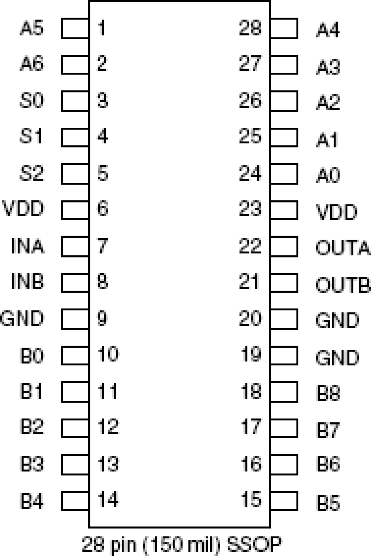
| Pkg. Type: | QSOP |
| Pkg. Code: | PCG28 |
| Lead Count (#): | 28 |
| Pkg. Dimensions (mm): | 9.9 x 3.8 x 1.47 |
| Pitch (mm): | 0.64 |
环境和出口类别
| Moisture Sensitivity Level (MSL) | 1 |
| Pb (Lead) Free | Yes |
| ECCN (US) | EAR99 |
| HTS (US) | 8542.39.0090 |
产品属性
| Lead Count (#) | 28 |
| Carrier Type | Tube |
| Moisture Sensitivity Level (MSL) | 1 |
| Qty. per Reel (#) | 0 |
| Qty. per Carrier (#) | 48 |
| Pb (Lead) Free | Yes |
| Pb Free Category | e3 Sn |
| Temp. Range (°C) | -40 to 85°C |
| Core Voltage (V) | 5 |
| Divider Value | 1, 2, 4, 5, 6, 7, 8, 10 |
| Function | Buffer, Divider |
| Input Freq (MHz) | 200, 235 |
| Input Type | LVCMOS |
| Inputs (#) | 2 |
| Length (mm) | 9.9 |
| MOQ | 2544 |
| Output Banks (#) | 2 |
| Output Freq Range (MHz) | 200, 235 |
| Output Type | LVCMOS |
| Output Voltage (V) | 5 |
| Outputs (#) | 2 |
| Package Area (mm²) | 37.6 |
| Pitch (mm) | 0.64 |
| Pkg. Dimensions (mm) | 9.9 x 3.8 x 1.47 |
| Pkg. Type | QSOP |
| Requires Terms and Conditions | Does not require acceptance of Terms and Conditions |
| Tape & Reel | No |
| Thickness (mm) | 1.47 |
| Width (mm) | 3.8 |
| 已发布 | No |
有关 674-01 的资源
描述
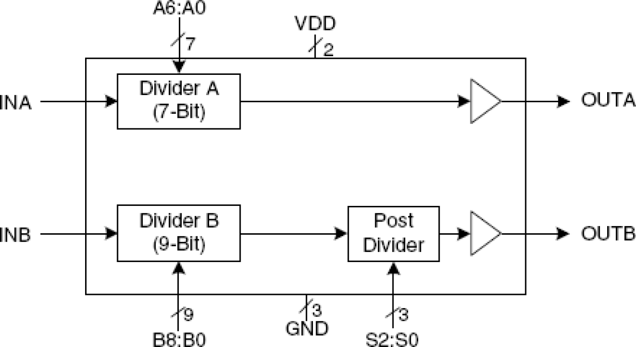
The 674-01 consists of two separate configurable dividers. The A Divider is a 7-bit divider and can divide by 3 to 129. The B Divider consists of a 9-bit divider followed by a post divider. The 9-bit divider can divide by 12 to 519. The post divider has eight settings of 1, 2, 4, 5, 6, 7, 8, and 10; giving a maximum total divide of 5190. The A and B Dividers can be cascaded to give a maximum divide of 669510. The 674-01 supports the 673 PLL Building Block and enables the user to build a full custom PLL synthesizer.

