特性
- DIF cycle-to-cycle jitter < 50ps
- DIF output-to-output skew < 50ps
- DIF phase jitter is PCIe Gen 1-2-3 compliant
- Very-low additive phase jitter in bypass mode
- Integrated terminations provide 100Ω differential Zo reduced component count and board space
- 1.8V operation; minimal power consumption
- Outputs can optionally be supplied from any voltage between 1.05V and 1.8V; maximum power savings
- OE# pins; support DIF power management
- HCSL-compatible differential input; can be driven by common clock sources
- LP-HCSL differential clock outputs; reduced power and board space
- Programmable slew rate for each output; allows tuning for various line lengths
- Programmable output amplitude; allows tuning for various application environments
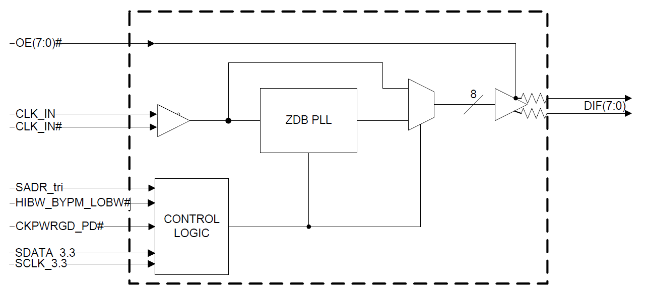
- Pin/Software selectable PLL bandwidth and PLL Bypass; minimize phase jitter for each application
- Outputs are blocked until PLL is locked; clean system start-up
- Software selectable 50MHz or 125MHz PLL operation; useful for Ethernet applications
- Configuration can be accomplished with strapping pins; SMBus interface is not required for device control
- 3.3V tolerant SMBus interface works with legacy controllers
- Space saving 48-pin 6mm x 6mm VFQFPN; minimal board space
- Selectable SMBus addresses; multiple devices can easily share an SMBus segment
描述
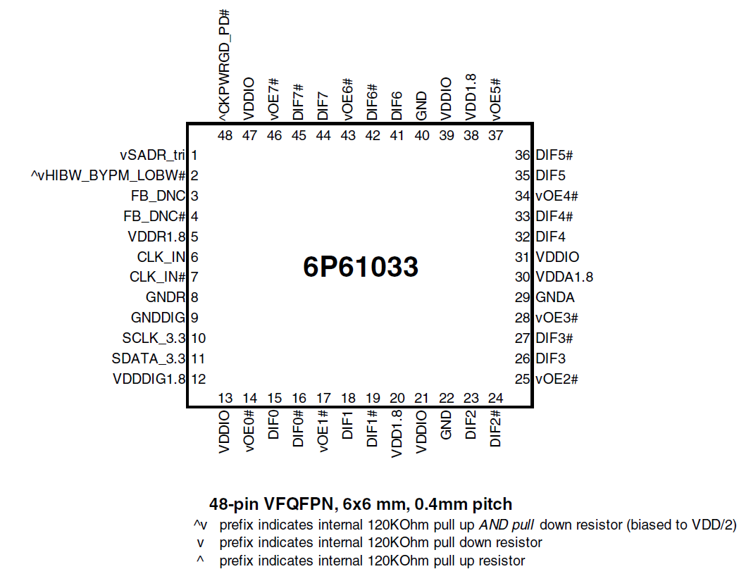
The 6P61033 is an 8-output very-low power buffer for 100MHz PCIe Gen 1, Gen 2, and Gen 3 applications with integrated output terminations providing Zo = 100Ω. The device has eight output enables for clock management and three selectable SMBus addresses.
| Part Number | Status | Samples | Stock | Package | Lead Count (#) | Carrier Type | Moisture Sensitivity Level (MSL) | Qty. per Reel (#) | Qty. per Carrier (#) | Pb (Lead) Free | Pb Free Category | Temp. Range (°C) |
|---|---|---|---|---|---|---|---|---|---|---|---|---|
| 6P61033NDGI | Obsolete | N/A | Out of Stock | VFQFPN | 48# | Tray | 3 | 0 | 490# | Yes | e3 Sn | -40 to 85°C |
| 6P61033NDGI8 | Obsolete | N/A | Out of Stock | VFQFPN | 48# | Reel | 3 | 2500# | 0 | Yes | e3 Sn | -40 to 85°C |
- 应用说明英语PDF 431 KB 7WDXRDKU4E7E-5-59216 2023年12月06日
- 应用说明英语PDF 495 KB 7WDXRDKU4E7E-5-57312 2014年5月12日
- 应用说明英语PDF 120 KB 7WDXRDKU4E7E-5-57289 2014年5月06日
- 应用说明英语PDF 160 KB 7WDXRDKU4E7E-5-57287 2014年5月06日
- EOL 通告英语PDF 550 KB 7WDXRDKU4E7E-5-58647 2015年3月11日
推荐文档 (1)
数据手册 (1)
No Results Found.
确保所有关键词拼写正确。
尝试使用更少、不同或更宽泛的词语来改变搜索结果。
如果您使用了筛选器,请考虑取消选择某些筛选器选项以扩大搜索结果。
- 搜索我们丰富的知识库,帮助您解答常见问题
- 前往支持论坛,获取瑞萨电子技术专家和社群的帮助
- 应用说明英语PDF 431 KB 7WDXRDKU4E7E-5-59216 2023年12月06日
应用说明和白皮书 (12)
- EOL 通告英语PDF 550 KB 7WDXRDKU4E7E-5-58647 2015年3月11日
产品通告(产品变更、EOL 等) (2)
No Results Found.
确保所有关键词拼写正确。
尝试使用更少、不同或更宽泛的词语来改变搜索结果。
如果您使用了筛选器,请考虑取消选择某些筛选器选项以扩大搜索结果。
- 搜索我们丰富的知识库,帮助您解答常见问题
- 前往支持论坛,获取瑞萨电子技术专家和社群的帮助
No Results Found.
确保所有关键词拼写正确。
尝试使用更少、不同或更宽泛的词语来改变搜索结果。
如果您使用了筛选器,请考虑取消选择某些筛选器选项以扩大搜索结果。
- 搜索我们丰富的知识库,帮助您解答常见问题
- 前往支持论坛,获取瑞萨电子技术专家和社群的帮助
No Results Found.
确保所有关键词拼写正确。
尝试使用更少、不同或更宽泛的词语来改变搜索结果。
如果您使用了筛选器,请考虑取消选择某些筛选器选项以扩大搜索结果。
- 搜索我们丰富的知识库,帮助您解答常见问题
- 前往支持论坛,获取瑞萨电子技术专家和社群的帮助
No Results Found.
确保所有关键词拼写正确。
尝试使用更少、不同或更宽泛的词语来改变搜索结果。
如果您使用了筛选器,请考虑取消选择某些筛选器选项以扩大搜索结果。
- 搜索我们丰富的知识库,帮助您解答常见问题
- 前往支持论坛,获取瑞萨电子技术专家和社群的帮助
No Results Found.
确保所有关键词拼写正确。
尝试使用更少、不同或更宽泛的词语来改变搜索结果。
如果您使用了筛选器,请考虑取消选择某些筛选器选项以扩大搜索结果。
- 搜索我们丰富的知识库,帮助您解答常见问题
- 前往支持论坛,获取瑞萨电子技术专家和社群的帮助
No Results Found.
确保所有关键词拼写正确。
尝试使用更少、不同或更宽泛的词语来改变搜索结果。
如果您使用了筛选器,请考虑取消选择某些筛选器选项以扩大搜索结果。
- 搜索我们丰富的知识库,帮助您解答常见问题
- 前往支持论坛,获取瑞萨电子技术专家和社群的帮助
营销资料 (1)
No Results Found.
确保所有关键词拼写正确。
尝试使用更少、不同或更宽泛的词语来改变搜索结果。
如果您使用了筛选器,请考虑取消选择某些筛选器选项以扩大搜索结果。
- 搜索我们丰富的知识库,帮助您解答常见问题
- 前往支持论坛,获取瑞萨电子技术专家和社群的帮助
No Results Found.
确保所有关键词拼写正确。
尝试使用更少、不同或更宽泛的词语来改变搜索结果。
如果您使用了筛选器,请考虑取消选择某些筛选器选项以扩大搜索结果。
- 搜索我们丰富的知识库,帮助您解答常见问题
- 前往支持论坛,获取瑞萨电子技术专家和社群的帮助
This is the first video in our PCIe series. In this video, we define PCIe architectures, focusing on common and separate clock architectures. Watch the rest of the video series below where Ron will cover the impact of different timing architectures.
In this episode, Ron Wade from IDT (acquired by Renesas) explains PCIe common clocking and its impact on timing solutions. Learn about using a single clock source, fan-out buffers, and the considerations for spread spectrum and non-spread spectrum clocking in PCIe systems.
In this video, we explore PCIe with separate reference clocks and the effects of clock selection. Learn how separate reference clocks work and their impact on system performance and stability.
This video provides a high-level overview of Separate Reference Clock with Independent Spread (SRIS) architectures for PCI Express systems, additional performance requirements that this clocking architecture imposes on the reference clocks, and some system implications encountered trying to implement the architecture.