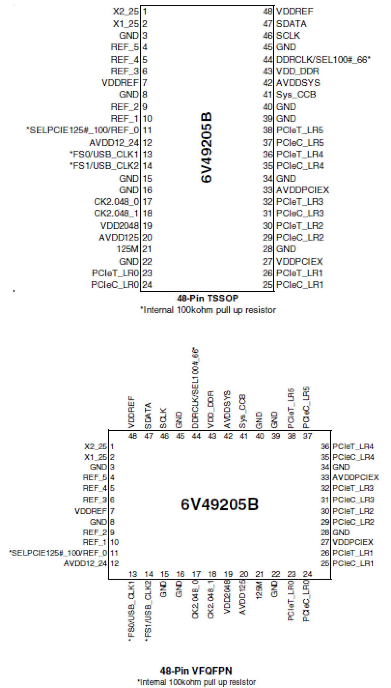
特性
- Packaged as a 48-pin TSSOP or 48-pin VFQFPN–Pb-free, RoHS-compliant
- Replaces 11 crystals, 2 oscillators, and 3 clock synthesizers
- Uses external reference crystal
- Operating voltage – 3.3V
- Supports spread spectrum modulation
- Supports I2C Standard and Fast modes
- Meets PCI Express Gen 1/2/3 performance
- 2.048MHz output to output skew <250ps
- Low phase noise for REF outputs
- Advanced, low-power CMOS process
- Supports the industrial temperature range
描述
The 6V49205B is a clock generator specifically designed for the Freescale P1010, P1020, P2020, and P2040 processors. The device uses a low-cost 25MHz crystal as an input and generates 19 high-quality output clocks for use in Freescale-based systems. The 6V49205B produces the following output frequencies:
- 1 – 100MHz/66.66MHz/80MHz/83.333MHz selectable for System CCB
- 1 – DDR_CLK; selectable 100MHz or 66.66MHz
- 2 – 12MHz/24MHz selectable outputs for USB
- 6 – PCIe differential low-power push-pull pairs; selectable 100MHz or 125MHz
- 6 – REF, 25MHz
- 2 – 2.048MHz for E1
- 1 – 125MHz for Gigabit
产品参数
属性 | 值 |
---|---|
Chipset Manufacturer | NXP |
Advanced Features | Programmable Clock, Spread Spectrum |
App Jitter Compliance | PCIe Gen1, PCIe Gen2, PCIe Gen3 |
Supply Voltage (V) | - |
Output Type | LVCMOS, HCSL |
Xtal Freq (MHz) | - |
Package Area (mm²) | 49, 76.3 |
应用
- System clock for Freescale P10xx and P20xx-based designs
当前筛选条件
筛选
软件与工具
样例程序
模拟模型
IDT provides a brief overview of the timing solutions optimized for various configurations using the NXP (Freescale) QorIQ / Layerscape processors.
Presented by Ron Wade, PCI Express timing expert. For more information about IDT's timing solutions, visit www.IDT.com/go/clocks.
TRANSCRIPT
So, hi there, this is Ron Wade again and we're going to be talking about timing solutions that IDT has for NXP's QorIQ and Layerscape CPU. And in the middle here, what I've drawn, in the middle of the box here, is what I refer to as our all-in-one solutions. These are single chips that may have all the clocks you need to build your system around the NXP CPUs. So, the three parts I have listed here are the 6P49V205, the 5P49V5907, and 5P49V5908. These provide a mix of the clocks that were needed over here for the CPU cores and SerDes clocks, and they're all on a single chip. If these suit your needs, these are ideal, these are the smallest core footprint parts to use.
The other approach besides all-in-one is the building block approach, and I'm going to start over here on the left side with the CPU clocks and the memory controller. For this solution over here, we have the 5P49V5901, or it could be a 6901, depending on your requirements. And, this guy has the most flexibility as far as programming up any combination of DDR clock or CPU clock that you want, as well as the 24 MHz USB clock and a 125 MHz clock.
If you're using the Layerscape CPU with the reduced oscillator mode where you have the 100 MHz non-spread clock coming in, you might want to consider the 9FGV0 series or the 9FGL0 series. These are very high-performance PCI Express clock generators, the V being a 1.8 volt part and the L being a 3.3 volt part that are available. The terminations are integrated, they're very low power and they also have some extra copies in case SerDes is a PCI Express SerDes. So, this is the ideal solution if you want to go building block over here.
And then for the SerDes clocks, we've got the 125 MHz differential for Gigabit Ethernet, the 156 MHz for 10 gig, and the 100 MHz for PCIe. We have again a different set of flavors we can go with. We have the 5P49V6901, which is a better performing, lower phase jitter version of the 5901 over here. This guy's ideal if you have a mix of these SerDes frequencies in your design. If you're in a homogeneous environment, for instance, where everything's PCI Express or everything is 125 MHz, then you could use the 9FGV parts, or I'll use an output from over there, over on this side for the 100 MHz output, or you could use these guys programmed up to be 125 as well. Or if you've got a 125 coming from over there, you can use one of the 9DVD buffers which are the 1.8V buffers to fan that out. Likewise, we have similar parts with 3.3-volt power supplies, if that's what you prefer. The 9FGL0 series, it should give you the 100 to the 125, and the 9DVL0 series which can provide a fanout buffer for any of these three frequencies.
So, that's an overview of the timing solutions for NXP's QorIQ and Layerscape CPUs. This is Ron Wade at IDT again. Thanks for watching and see you next time.
IDT provides a brief tutorial on the timing solutions required for NXP (Freescale) QorIQ / Layerscape processor-based systems.
Presented by Ron Wade, PCI Express timing expert. For more information about IDT's timing solutions, visit www.IDT.com/go/clocks.
TRANSCRIPT
Hi there, this is Ron Wade with IDT and today we're going to talk about NXP, formerly known as Freescale, CPUs. Specifically the QorIQ and Layerscape CPUs and the timing requirements that they have. So, it's basically divided into a couple of parts here. There's some timing that the CPU itself requires and then there's timing that depends upon your system and the number of SerDes links you have in your design and in your CPU. So, if we talk about the CPU part itself, we have the CPU cores which get a clock, and we have the memory controller inside the CPUs which gets a clock as well. And the memory controller clock is called the DDR clock. The CPU clock is called the SYS_CCB clock in the Freescale nomenclature, excuse me, the NXP nomenclature and those frequencies - they're single-ended clocks and they range, like the DDR from 66.66 MHz up to 100 MHz, and the CPU clocks range from 66.66 up to 133.33 MHz, in some cases. Those are single-ended LVCMOS input clocks. Additionally, some of the CPUs have a USB interface which may require a 24 MHz single-ended clock. And there's also an Ethernet interface built in, a one-gigabit Ethernet interface, that is, takes a 125 MHz single-ended clock as well and that's at 2.5 volts.
So, in the Layerscape series of CPUs which are based on the ARM core, Freescale has put into them, what they call a reduced oscillator mode where all the clocks over here basically are reduced by a single differential 100 MHz non-spreading clock, and this saves you from having to figure out and generate all these clocks. However, it has to be non-spread because the USB clock is also derived from it, so, if you're planning to use spread spectrum, you really can't use this mode. And, currently, it's only available in the Layerscape devices, not the legacy QorIQ devices.
So, that's the basics for the CPU and the memory controller. Then the SerDes is really dependent upon the particular CPU you're using and how many SerDes lanes you need in your design. So, the SerDes clocks, on the other hand, basically range from 125 MHz differential clock for Gigabit Ethernet, if you're using 10 Gigabit Ethernet, a 156.25 MHz clock is required. And then if you're using PCI Express, you'd use a standard 100 MHz PCI Express clock. All these happen to be differential and the number of SerDes lanes and their capabilities depends on the CPU you're using. So, this gives you an outline of how to just do a quick tally of what kind of clocks you need and in another video, I'll talk about the solutions that IDT has for NXP's devices.