| CAD 模型: | View CAD Model |
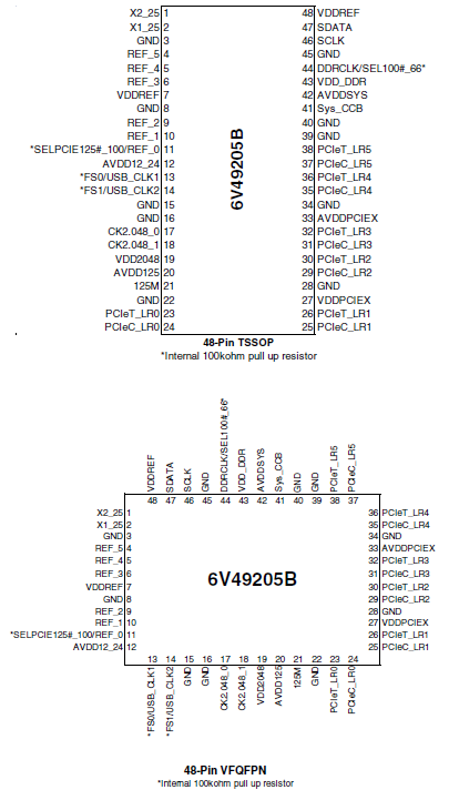
| Pkg. Type: | VFQFPN |
| Pkg. Code: | NLG48 |
| Lead Count (#): | 48 |
| Pkg. Dimensions (mm): | 7.0 x 7.0 x 0.9 |
| Pitch (mm): | 0.5 |
| Moisture Sensitivity Level (MSL) | 3 |
| Pb (Lead) Free | Yes |
| ECCN (US) | EAR99 |
| HTS (US) | 8542.39.0090 |
| Lead Count (#) | 48 |
| Carrier Type | Tray |
| Moisture Sensitivity Level (MSL) | 3 |
| Qty. per Carrier (#) | 260 |
| Package Area (mm²) | 49 |
| Pkg. Dimensions (mm) | 7.0 x 7.0 x 0.9 |
| Qty. per Reel (#) | 0 |
| Pb (Lead) Free | Yes |
| Pb Free Category | e3 Sn |
| Temp. Range (°C) | -40 to 85°C |
| Country of Assembly | TAIWAN |
| Country of Wafer Fabrication | TAIWAN |
| Advanced Features | Programmable Clock, Spread Spectrum |
| App Jitter Compliance | PCIe Gen1, PCIe Gen2, PCIe Gen3 |
| Architecture | Common |
| C-C Jitter Max P-P (ps) | 50 |
| C-C Jitter Typ P-P (ps) | 35 |
| Chipset Manufacturer | NXP |
| Chipset Name | P1010, P1020, P2020, P2040 |
| Core Voltage (V) | 3.3V |
| Function | Generator |
| Input Freq (MHz) | 25 - 25 |
| Input Type | Crystal, LVCMOS |
| Inputs (#) | 1 |
| Length (mm) | 7 |
| MOQ | 260 |
| NXP Processor Function | Memory Clock, SerDes Clock, CPU/USB/Eth Clock |
| Output Banks (#) | 8 |
| Output Freq Range (MHz) | 100 - 100, 66.66 - 66.66, 80 - 80, 83.333 - 83.333, 12 - 12, 24 - 24, 125 - 125, 2.048 - 2.048, 25 - 25 |
| Output Skew (ps) | 50 |
| Output Type | LVCMOS, HCSL |
| Output Voltage (V) | 0.8V, 3.3V |
| Outputs (#) | 19 |
| Period Jitter Max P-P (ps) | 150 |
| Phase Jitter Max RMS (ps) | 0.2 |
| Phase Jitter Typ RMS (ps) | 0.11 |
| Pitch (mm) | 0.5 |
| Pkg. Type | VFQFPN |
| Price (USD) | $3.21106 |
| Prog. Clock | No |
| Prog. Interface | SMBUS |
| Reference Output | No |
| Requires Terms and Conditions | Does not require acceptance of Terms and Conditions |
| Spread Spectrum | Yes |
| Supply Voltage (V) | 3.3 - 3.3 |
| Tape & Reel | No |
| Thickness (mm) | 0.9 |
| Width (mm) | 7 |
| Xtal Freq (MHz) | 25 - 25 |
| 已发布 | No |
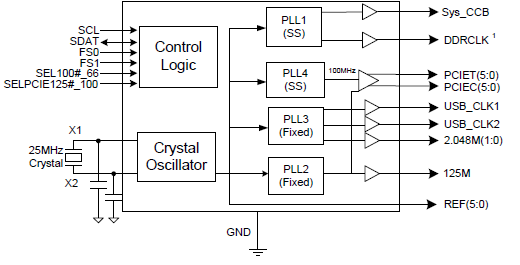
The 6V49205B is a clock generator specifically designed for the Freescale P1010, P1020, P2020, and P2040 processors. The device uses a low-cost 25MHz crystal as an input and generates 19 high-quality output clocks for use in Freescale-based systems. The 6V49205B produces the following output frequencies: