
| CAD 模型: | View CAD Model |
| Pkg. Type: | SOT |
| Pkg. Code: | DYG6 |
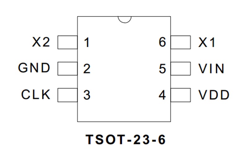
| Lead Count (#): | 6 |
| Pkg. Dimensions (mm): | 2.9 x 1.6 x 1.0 |
| Pitch (mm): | 0.95 |
| Moisture Sensitivity Level (MSL) | 1 |
| Pb (Lead) Free | Yes |
| ECCN (US) | EAR99 |
| HTS (US) | 8542.39.0090 |
| Lead Count (#) | 6 |
| Carrier Type | Can |
| Moisture Sensitivity Level (MSL) | 1 |
| Qty. per Reel (#) | 0 |
| Pb (Lead) Free | Yes |
| Pb Free Category | e3 Sn |
| Temp. Range (°C) | 0 to 70°C |
| Accepts Spread Spec Input | No |
| Core Voltage (V) | 3.3 |
| Feedback Input | No |
| Input Freq (MHz) | 12 - 36 |
| Input Type | Crystal, LVCMOS |
| Inputs (#) | 2 |
| Length (mm) | 2.9 |
| MOQ | 500 |
| Output Banks (#) | 1 |
| Output Freq Range (MHz) | 12 - 36 |
| Output Signaling | CMOS |
| Output Type | LVCMOS |
| Output Voltage (V) | 3.3 |
| Outputs (#) | 1 |
| Package Area (mm²) | 4.6 |
| Period Jitter Typ P-P (ps) | 100 |
| Pitch (mm) | 0.95 |
| Pkg. Dimensions (mm) | 2.9 x 1.6 x 1.0 |
| Pkg. Type | SOT |
| Product Category | General Purpose Clocks |
| Prog. Clock | No |
| Qty. per Carrier (#) | 0 |
| Reference Output | No |
| Requires Terms and Conditions | Does not require acceptance of Terms and Conditions |
| Spread Spectrum | No |
| Supply Voltage (V) | 3.3 - 3.3 |
| Tape & Reel | No |
| Thickness (mm) | 1 |
| Width (mm) | 1.6 |
| Xtal Freq (KHz) | 12 - 36 |
| Xtal Inputs (#) | 1 |
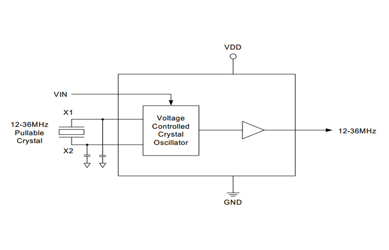
Used in conjunction with an external pullable quartz crystal, this monolithic integrated circuit replaces more costly hybrid (canned) VCXO devices. The IDT726A is designed primarily for data and clock recovery applications such as ADSL modems, set-top box receivers, and telecom systems. The frequency of the on-chip VCXO is adjusted by an external control voltage to the VIN pin. Since VIN is a high impedance input, it can be driven directly from an PWM RC integrator circuit. Frequency output increases with VIN voltage input. The usable range of VIN is 0 to 3.3 V.