封装信息
| CAD 模型: | View CAD Model |
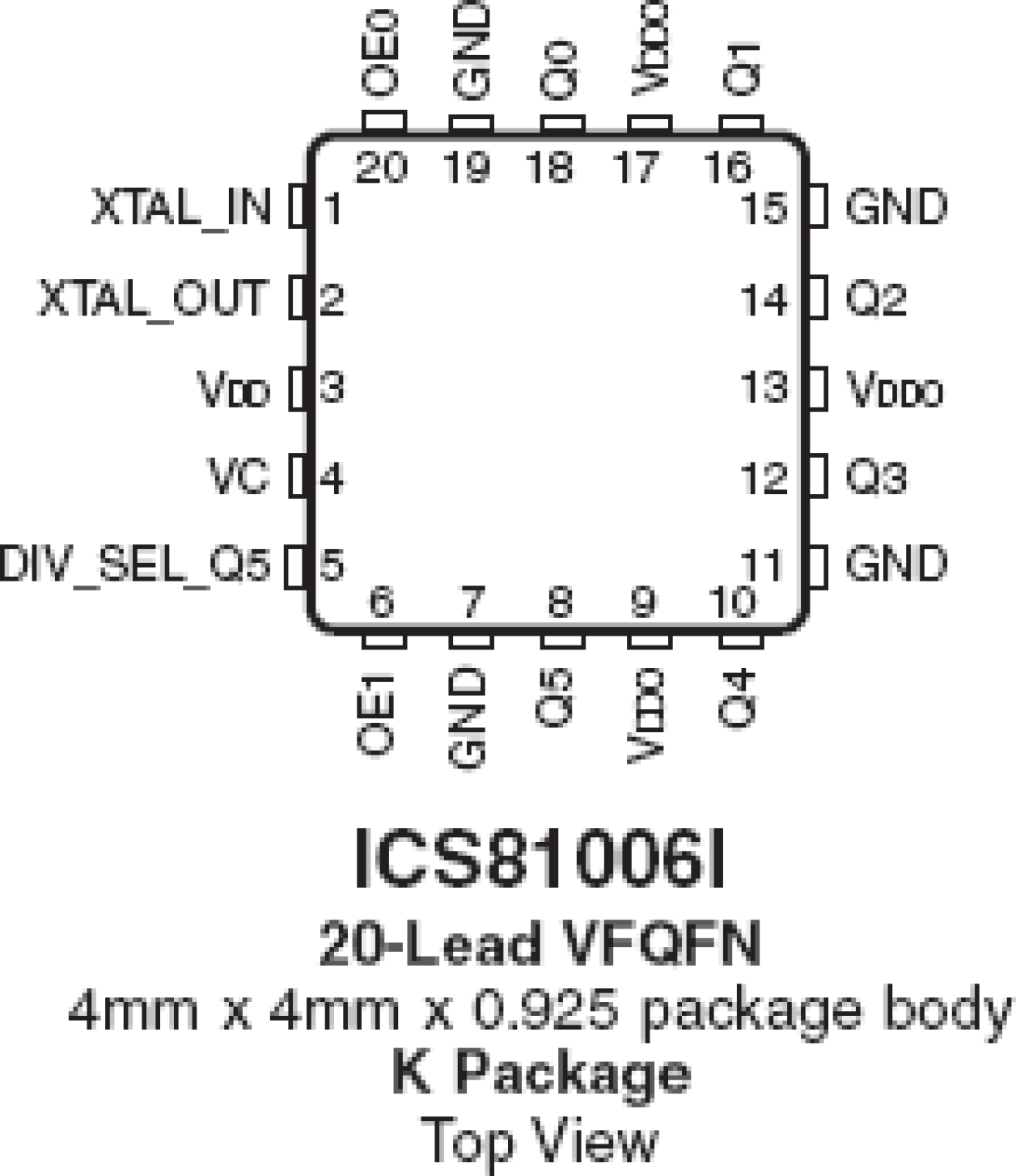
| Pkg. Type: | VFQFPN |
| Pkg. Code: | NLG20 |
| Lead Count (#): | 20 |
| Pkg. Dimensions (mm): | 4.0 x 4.0 x 1.0 |
| Pitch (mm): | 0.5 |
环境和出口类别
| Moisture Sensitivity Level (MSL) | 1 |
| Pb (Lead) Free | Yes |
| ECCN (US) | EAR99 |
| HTS (US) | 8542.39.0090 |
产品属性
| Lead Count (#) | 20 |
| Carrier Type | Reel |
| Moisture Sensitivity Level (MSL) | 1 |
| Qty. per Reel (#) | 2500 |
| Qty. per Carrier (#) | 0 |
| Pb (Lead) Free | Yes |
| Pb Free Category | e3 Sn |
| Temp. Range (°C) | -40 to 85°C |
| Core Voltage (V) | 2.5V, 3.3V |
| Divider Value | 1, 2 |
| Function | Buffer, Divider |
| Input Freq (MHz) | 12 - 31.25 |
| Input Type | LVCMOS |
| Inputs (#) | 1 |
| Length (mm) | 4 |
| MOQ | 2500 |
| Output Banks (#) | 2 |
| Output Freq Range (MHz) | 12 - 31.25 |
| Output Skew (ps) | 20 |
| Output Type | LVCMOS |
| Output Voltage (V) | 1.8V, 2.5V, 3.3V |
| Outputs (#) | 6 |
| Package Area (mm²) | 16 |
| Pitch (mm) | 0.5 |
| Pkg. Dimensions (mm) | 4.0 x 4.0 x 1.0 |
| Pkg. Type | VFQFPN |
| Reel Size (in) | 13 |
| Requires Terms and Conditions | Does not require acceptance of Terms and Conditions |
| Tape & Reel | Yes |
| Thickness (mm) | 1 |
| Width (mm) | 4 |
| 已发布 | No |
有关 81006I 的资源
描述
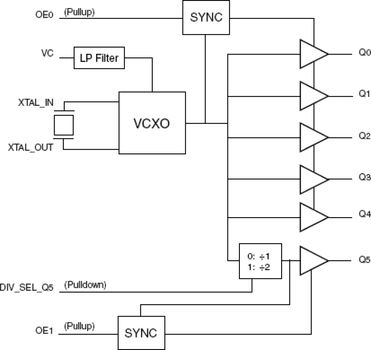
The 81006I is a high performance, low jitter/ low phase noise VCXO and is a member of the family of high performance clock solutions from IDT. The 81006I works in conjunction with a pullable crystal to generate an output clock over the range of 12MHz - 31.25MHz and has 6 LVCMOS outputs, effectively integrating a fanout buffer function.
The frequency of the VCXO is adjusted by the VC control voltage input. The output range is ±100ppm around the nominal crystal frequency. The VC control voltage range is 0 - VDD. The device is packaged in a small 4mm x 4mm VFQFN package and is ideal for use on space constrained boards typically encountered in ADSL/VDSL applications.

