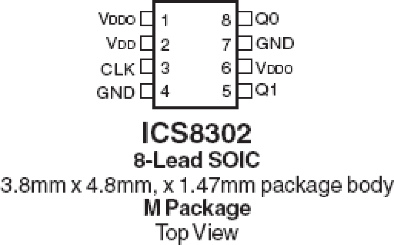
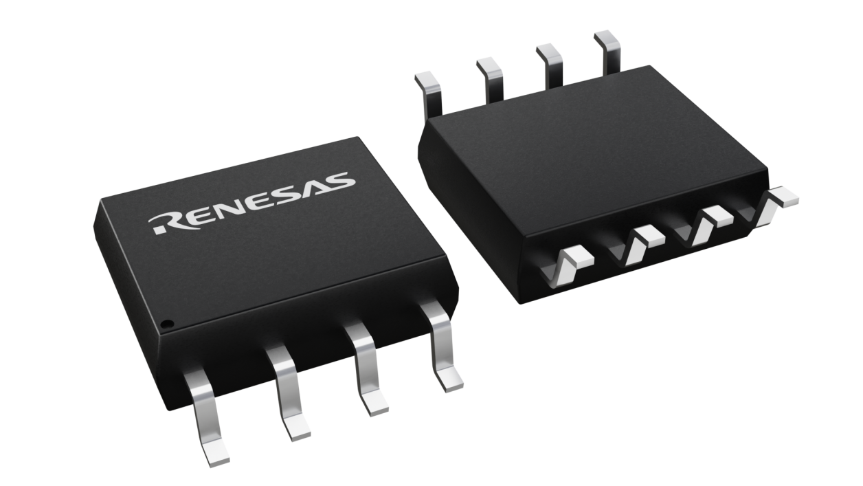
封装信息
| CAD 模型: | View CAD Model |
| Pkg. Type: | SOIC |
| Pkg. Code: | DCG8 |
| Lead Count (#): | 8 |
| Pkg. Dimensions (mm): | 4.9 x 3.9 x 1.5 |
| Pitch (mm): | 1.27 |
环境和出口类别
| Moisture Sensitivity Level (MSL) | 1 |
| Pb (Lead) Free | Yes |
| ECCN (US) | EAR99 |
| HTS (US) | 8542.39.0090 |
产品属性
| Lead Count (#) | 8 |
| Carrier Type | Tube |
| Moisture Sensitivity Level (MSL) | 1 |
| Qty. per Reel (#) | 0 |
| Qty. per Carrier (#) | 97 |
| Pb (Lead) Free | Yes |
| Pb Free Category | e3 Sn |
| Temp. Range (°C) | 0 to 70°C |
| Core Voltage (V) | 3.3 |
| Function | Buffer |
| Input Freq (MHz) | 200 |
| Input Type | LVCMOS |
| Inputs (#) | 1 |
| Length (mm) | 4.9 |
| MOQ | 194 |
| Output Banks (#) | 1 |
| Output Freq Range (MHz) | 200 |
| Output Skew (ps) | 85 |
| Output Type | LVCMOS |
| Output Voltage (V) | 2.5V, 3.3V |
| Outputs (#) | 2 |
| Package Area (mm²) | 19.1 |
| Pitch (mm) | 1.27 |
| Pkg. Dimensions (mm) | 4.9 x 3.9 x 1.5 |
| Pkg. Type | SOIC |
| Product Category | Clock Buffers & Drivers |
| Requires Terms and Conditions | Does not require acceptance of Terms and Conditions |
| Tape & Reel | No |
| Thickness (mm) | 1.5 |
| Width (mm) | 3.9 |
| 已发布 | No |
有关 8302 的资源
描述
The 8302 is a low skew, 1-to-2 LVCMOS/LVTTL Fanout Buffer. The 8302 has a single-ended clock input. The single-ended clock input accepts LVCMOS or LVTTL input levels. The 8302 features a pair of LVCMOS/LVTTL outputs. The 8302 is characterized at full 3.3V for input VDD, and mixed 3.3V and 2.5V for output operating supply modes (VDDO). Guaranteed output and part-to-part skew characteristics make the 8302 ideal for clock distribution applications demanding well-defined performance and repeatability.


