特性
- Fourth generation FemtoClock NG technology
- 106.25MHz output clock synthesized from a 26.5625MHz fundamental mode crystal
- One 2.5V or 3.3V LVCMOS/LVTTL clock output
- Crystal interface designed for a 12pF parallel resonant crystal
- RMS phase jitter at 100MHz, using a 25MHz crystal (637kHz to 10MHz): 0.185ps (maximum)
- LVCMOS/LVTTL interface level for the output enable input
- Full 2.5V or 3.3V supply voltage
- Lead-free (RoHS 6) packaging
- -40 °C to 85 °C ambient operating temperature
描述
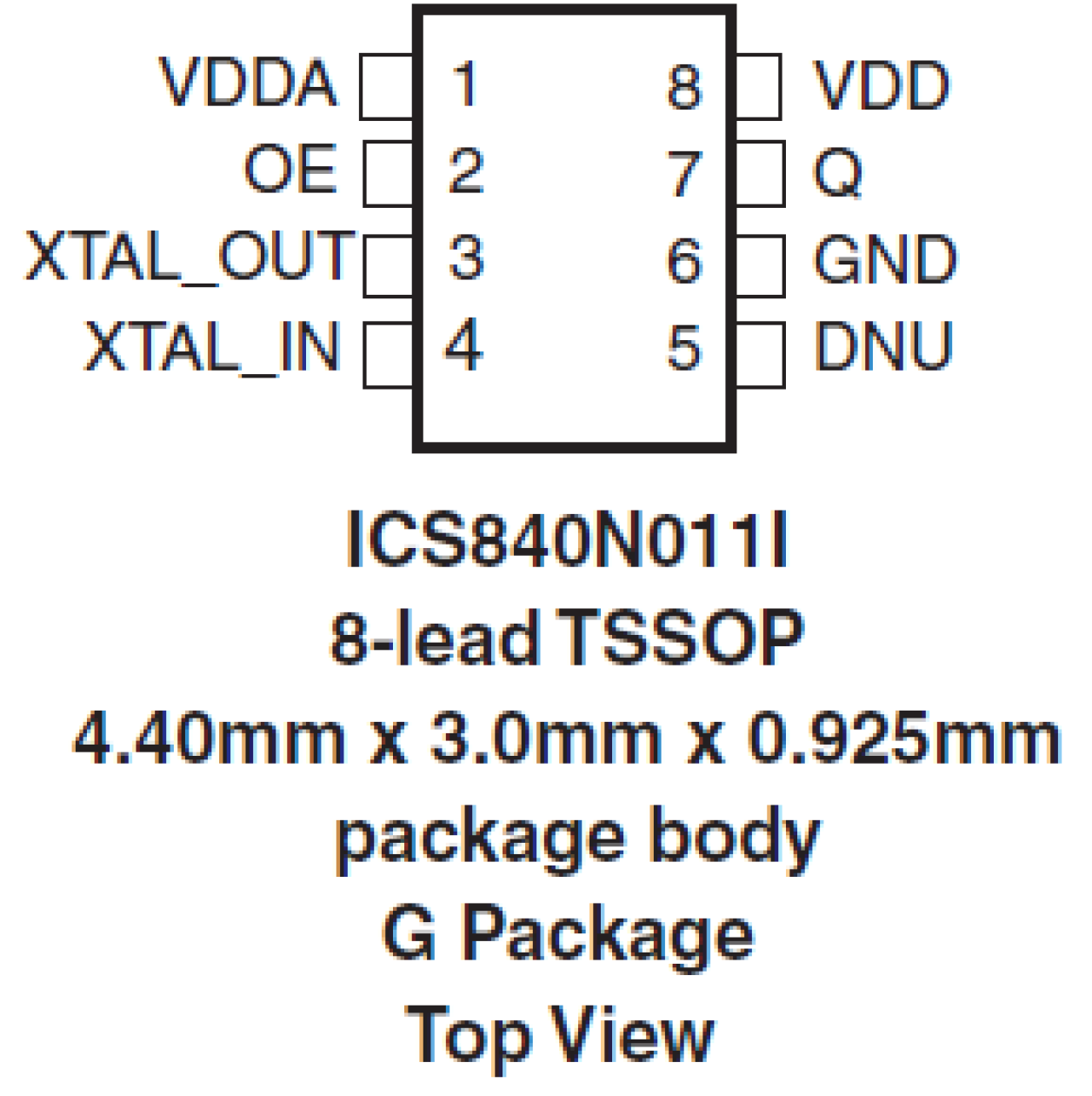
The 840N011I is an LVCMOS/LVTTL clock synthesizer designed for Fibre Channel applications. The device generates a 106.25MHz clock signal from a 26.5625MHz crystal or a 100MHz clock signal from a 25MHz crystal with excellent phase jitter performance. The 840N011I uses Renesas' fourth generation FemtoClock® NG technology for an optimum of high clock frequency, low phase noise performance and low power consumption, and high power supply noise rejection.The device supports 2.5V or 3.3V voltage supply and is packaged in a small, lead-free (RoHS 6) 8-lead TSSOP package. The extended temperature range supports wireless infrastructure, telecommunication, and networking end equipment requirements.
当前筛选条件


