封装信息
| CAD 模型: | View CAD Model |
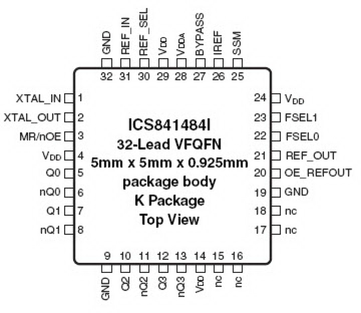
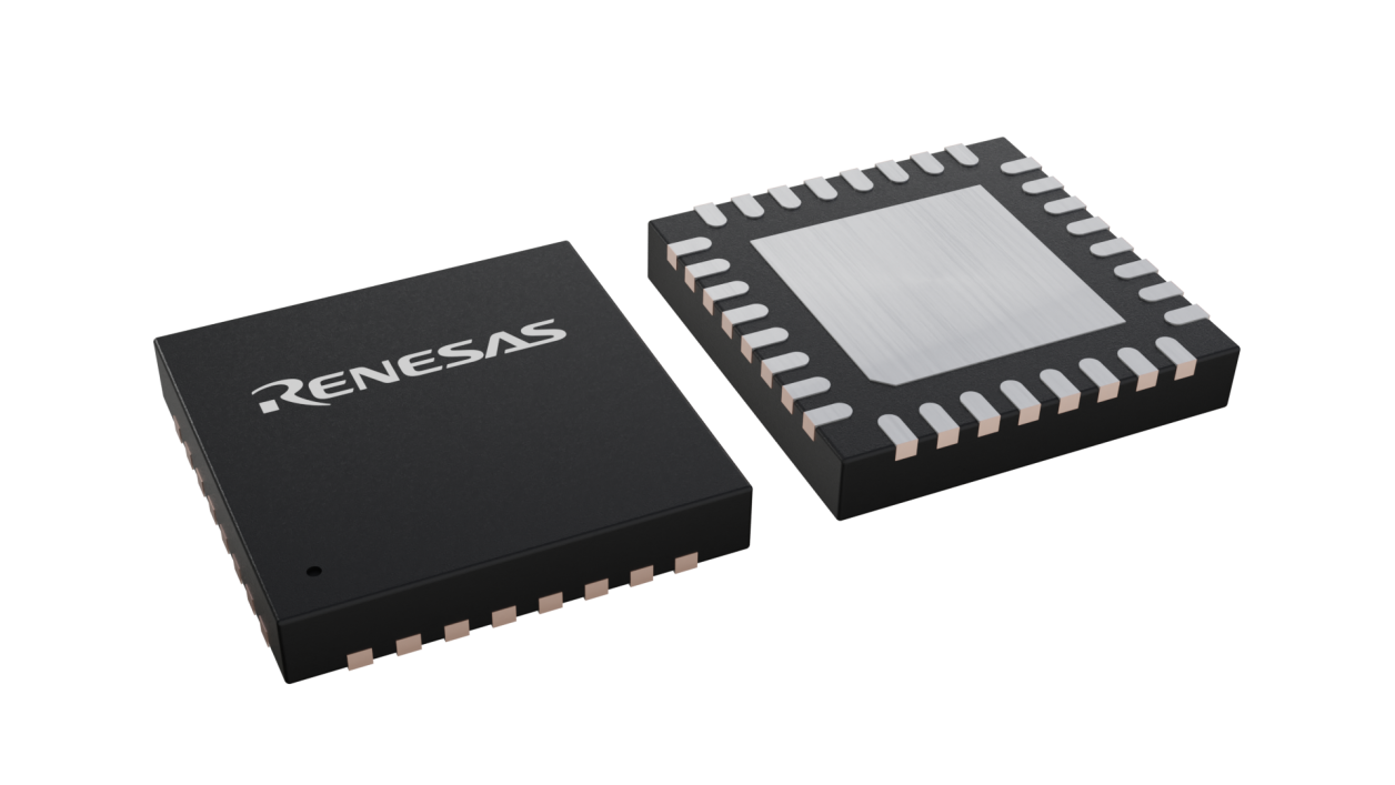
| Pkg. Type: | VFQFPN |
| Pkg. Code: | NLG32 |
| Lead Count (#): | 32 |
| Pkg. Dimensions (mm): | 5.0 x 5.0 x 0.9 |
| Pitch (mm): | 0.5 |
环境和出口类别
| Moisture Sensitivity Level (MSL) | 3 |
| Pb (Lead) Free | Yes |
| ECCN (US) | EAR99 |
| HTS (US) | 8542.39.0090 |
产品属性
| Lead Count (#) | 32 |
| Carrier Type | Tray |
| Moisture Sensitivity Level (MSL) | 3 |
| Qty. per Reel (#) | 0 |
| Qty. per Carrier (#) | 490 |
| Pb (Lead) Free | Yes |
| Pb Free Category | e3 Sn |
| Temp. Range (°C) | -40 to 85°C |
| Advanced Features | Spread Spectrum, Reference Output |
| App Jitter Compliance | PCIe Gen1, PCIe Gen2, PCIe Gen3 |
| Architecture | Common |
| C-C Jitter Max P-P (ps) | 36 |
| C-C Jitter Typ P-P (ps) | 15 |
| Core Voltage (V) | 3.3 |
| Diff. Output Signaling | HCSL |
| Diff. Outputs | 4 |
| Input Freq (MHz) | 25 - 25 |
| Input Type | Crystal, LVCMOS |
| Inputs (#) | 2 |
| Length (mm) | 5 |
| MOQ | 490 |
| Output Banks (#) | 2 |
| Output Freq Range (MHz) | 25 - 25, 100 - 100, 125 - 125, 200 - 200, 400 - 400 |
| Output Skew (ps) | 70 |
| Output Type | HCSL, LVCMOS |
| Output Voltage (V) | 3.3 |
| Outputs (#) | 5 |
| Package Area (mm²) | 25 |
| Phase Jitter Max RMS (ps) | 0.35 |
| Phase Jitter Typ RMS (ps) | 0.16 |
| Pitch (mm) | 0.5 |
| Pkg. Dimensions (mm) | 5.0 x 5.0 x 0.9 |
| Pkg. Type | VFQFPN |
| Prog. Clock | No |
| Reference Output | Yes |
| Requires Terms and Conditions | Does not require acceptance of Terms and Conditions |
| Spread Spectrum | Yes |
| Supply Voltage (V) | 3.3 - 3.3 |
| Tape & Reel | No |
| Thickness (mm) | 0.9 |
| Width (mm) | 5 |
| 已发布 | No |
有关 841484I 的资源
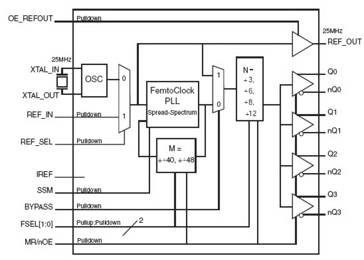
描述
The 841484I is an optimized PCIe and sRIO clock generator. The device uses a 25MHz parallel resonant crystal to generate 100MHz, 125MHz, 200MHz and 400MHz clock signals, replacing solutions requiring multiple oscillator and fanout buffer solutions. The device has excellent phase jitter suitable to clock components requiring precise and low jitter PCIe, sRIO or both clock signals. The device also supports a configurable spread-spectrum generation for PCIe applications. Designed for telecom, networking and industrial applications, the 841484I can also drive the high-speed sRIO and PCIe SerDes clock inputs of communications processors, DSPs, switches and bridges.


