特性
- Three LVDS outputs on two banks, A Bank with one LVDS pair and B Bank with two LVDS output pairs
- Using a 31.25MHz or 26.041666MHz crystal, the two output banks can be independently set for 625MHz, 312.5MHz, 156.25MHz, or 125MHz
- Selectable crystal oscillator interface or LVCMOS/LVTTL single-ended input
- VCO range: 560MHz to 700MHz
- RMS phase jitter at 156.25MHz (1.875MHz to 20MHz): 0.63ps (typical)
- 3.3V output supply mode
- 0 °C to 70 °C ambient operating temperature
- Available in lead-free (RoHS 6) packaging
描述
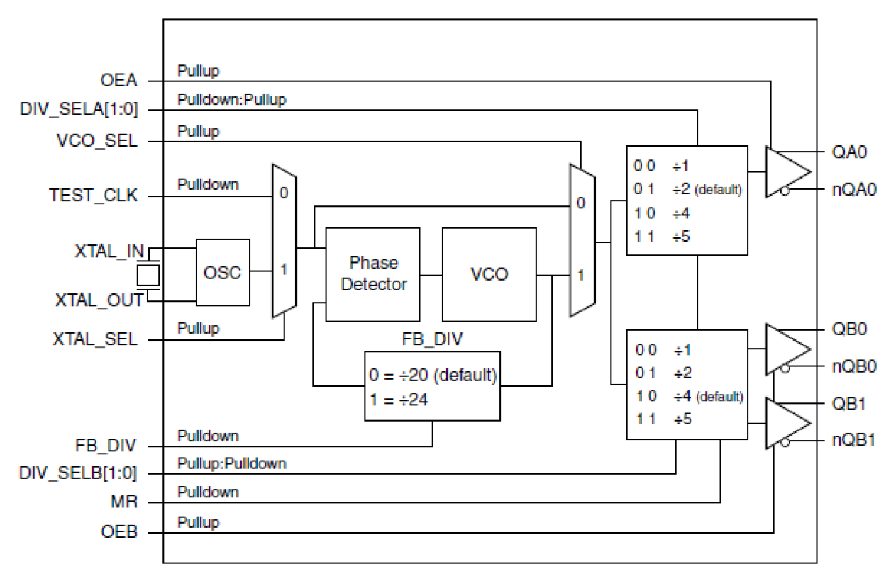
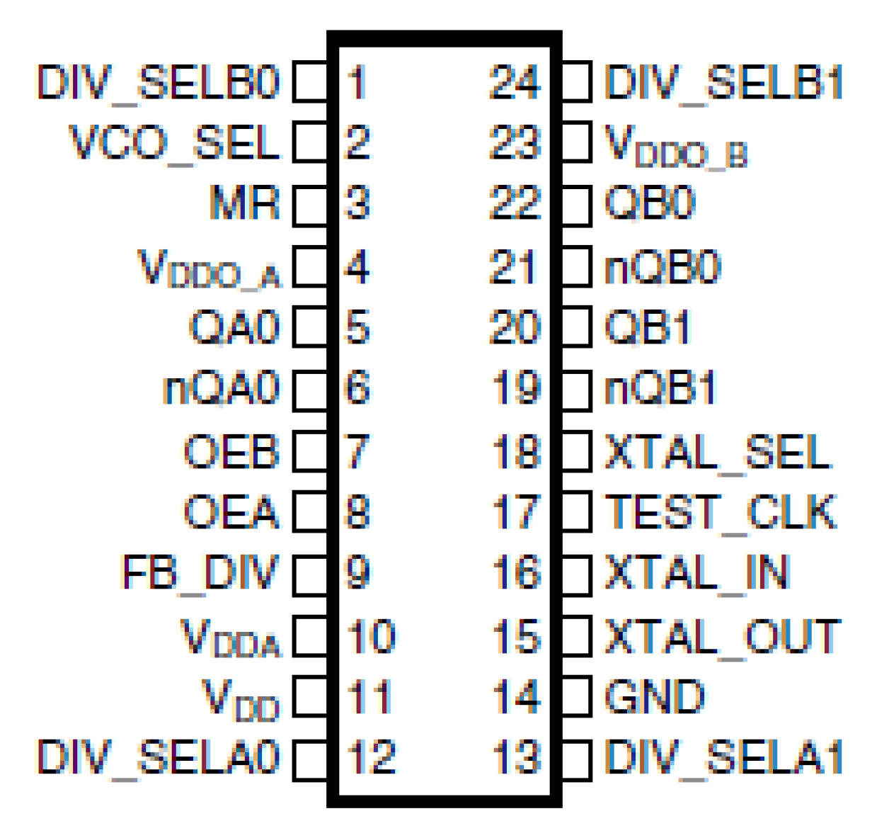
The 844003 is a three differential output LVDS synthesizer designed to generate Ethernet reference clock frequencies. Using a 31.25MHz or 26.041666MHz, 18pF parallel resonant crystal, the following frequencies can be generated based on the settings of four frequency select pins (DIV_SEL[A1:A0], DIV_SEL[B1:B0]): 625MHz, 312.5MHz, 156.25MHz, and 125MHz. The 844003 has two output banks, Bank A with one differential LVDS output pair and Bank B with two differential LVDS output pairs.
The two banks have their own dedicated frequency select pins and can be independently set for the frequencies mentioned above. The 844003 uses Renesas' third-generation low phase noise VCO technology and can achieve 1ps or lower typical RMS phase jitter, easily meeting Ethernet jitter requirements. The 844003 is packaged in a small 24-pin TSSOP package.
当前筛选条件


