
| CAD 模型: | View CAD Model |
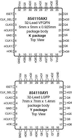
| Pkg. Type: | TQFP |
| Pkg. Code: | PRG32 |
| Lead Count (#): | 32 |
| Pkg. Dimensions (mm): | 7.0 x 7.0 x 1.4 |
| Pitch (mm): | 0.8 |
| Moisture Sensitivity Level (MSL) | 3 |
| Pb (Lead) Free | Yes |
| ECCN (US) | EAR99 |
| HTS (US) | 8542.39.0090 |
| Lead Count (#) | 32 |
| Carrier Type | Reel |
| Moisture Sensitivity Level (MSL) | 3 |
| Qty. per Reel (#) | 2000 |
| Qty. per Carrier (#) | 0 |
| Package Area (mm²) | 49 |
| Pitch (mm) | 0.8 |
| Pkg. Dimensions (mm) | 7.0 x 7.0 x 1.4 |
| Pb (Lead) Free | Yes |
| Pb Free Category | e3 Sn |
| Temp. Range (°C) | -40 to 85°C |
| Additive Phase Jitter Typ RMS (fs) | 291 |
| Additive Phase Jitter Typ RMS (ps) | 0.291 |
| Core Voltage (V) | 2.5 |
| Function | Buffer, Multiplexer |
| Input Freq (MHz) | 200 |
| Input Type | LVDS, LVPECL |
| Inputs (#) | 2 |
| Length (mm) | 7 |
| MOQ | 2000 |
| Output Banks (#) | 1 |
| Output Freq Range (MHz) | 200 |
| Output Skew (ps) | 260 |
| Output Type | LVDS |
| Output Voltage (V) | 2.5 |
| Outputs (#) | 10 |
| Pkg. Type | TQFP |
| Reel Size (in) | 13 |
| Requires Terms and Conditions | Does not require acceptance of Terms and Conditions |
| Tape & Reel | Yes |
| Thickness (mm) | 1.4 |
| Width (mm) | 7 |
| 已发布 | No |
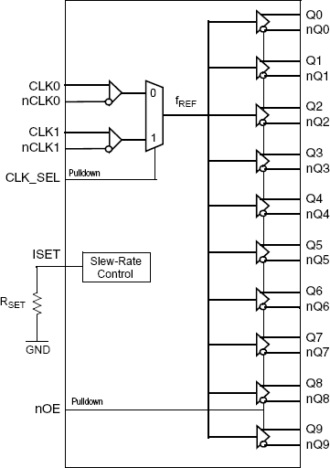
The 854110I is a high-performance differential LVDS clock fanout buffer. The device is designed for signal fanout of high-frequency, low phase-noise clock signals. The selected differential input signal is distributed to ten differential LVDS outputs. The 854110I is characterized to operate from a 2.5V power supply. Guaranteed output-to-output and part-to-part skew characteristics make the 854110I ideal for those clock distribution applications demanding well-defined performance and repeatability. The device offers an output slew rate control with four pre-set output transition times to solve crosstalk and EMI problems in complex board designs. A fail-safe input design forces the outputs to a defined state if differential clock inputs are open or shorted, see Table 3D.