
特性
- Three differential 3.3V LVPECL outputs
- Selectable differential clock inputs
- CLKx, nCLKx pairs can accept the following differential input levels: LVPECL, LVDS, LVHSTL, HCSL, SSTL
- Output frequency range: 31.25MHz to 700MHz
- Input frequency range: 31.25MHz to 700MHz
- VCO range: 250MHz to 700MHz
- External feedback for "zero delay" clock regeneration
- Cycle-to-cycle jitter: 25ps (maximum)
- Output skew: 25ps (maximum)
- PLL reference zero delay: 50ps ± 100ps
- 3.3V operating supply
- 0°C to 70°C ambient operating temperature
- Industrial temperature information available upon request
- Available in both standard and lead-free RoHs-compliant packages
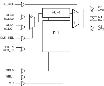
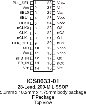
8633-01 - Block Diagram
描述
The 8633-01 is a high performance 1-to-3 Differential-to-3.3V LVPECL Zero Delay Buffer. The 8633-01 has two selectable clock inputs. The CLKx, nCLKx pairs can accept most standard differential input levels. Utilizing one of the outputs as feedback to the PLL, output frequencies up to 700MHz can be regenerated with zero delay with respect to the input. Dual reference clock inputs support redundant clock or multiple reference applications.


