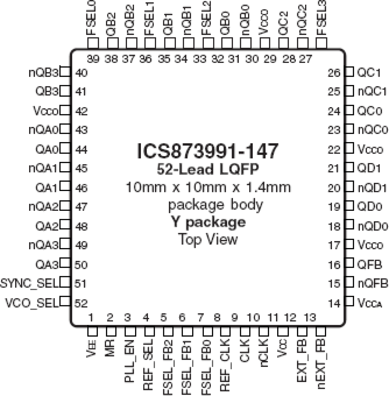
封装信息
| CAD 模型: | View CAD Model |
| Pkg. Type: | TQFP |
| Pkg. Code: | PPG52 |
| Lead Count (#): | 52 |
| Pkg. Dimensions (mm): | 10.0 x 10.0 x 1.4 |
| Pitch (mm): | 0.65 |
环境和出口类别
| Moisture Sensitivity Level (MSL) | 3 |
| Pb (Lead) Free | Yes |
| ECCN (US) | EAR99 |
| HTS (US) | 8542.39.0090 |
产品属性
| Lead Count (#) | 52 |
| Carrier Type | Tray |
| Moisture Sensitivity Level (MSL) | 3 |
| Qty. per Reel (#) | 0 |
| Qty. per Carrier (#) | 160 |
| Pb (Lead) Free | Yes |
| Pb Free Category | e3 Sn |
| Temp. Range (°C) | 0 to 70°C |
| Advanced Features | Feedback Input |
| C-C Jitter Max P-P (ps) | 50 |
| Core Voltage (V) | 3.3 |
| Feedback Input | Yes |
| Input Freq (MHz) | 6.25 - 120 |
| Input Type | HCSL, HSTL, LVDS, LVPECL, SSTL |
| Inputs (#) | 2 |
| Length (mm) | 10 |
| MOQ | 160 |
| Output Banks (#) | 4 |
| Output Freq Range (MHz) | 480 |
| Output Skew (ps) | 250 |
| Output Type | LVPECL |
| Output Voltage (V) | 3.3 |
| Outputs (#) | 13 |
| Package Area (mm²) | 100 |
| Pitch (mm) | 0.65 |
| Pkg. Dimensions (mm) | 10.0 x 10.0 x 1.4 |
| Pkg. Type | TQFP |
| Prog. Clock | No |
| Requires Terms and Conditions | Does not require acceptance of Terms and Conditions |
| Tape & Reel | No |
| Thickness (mm) | 1.4 |
| Width (mm) | 10 |
| 已发布 | No |
有关 873991-147 的资源
描述
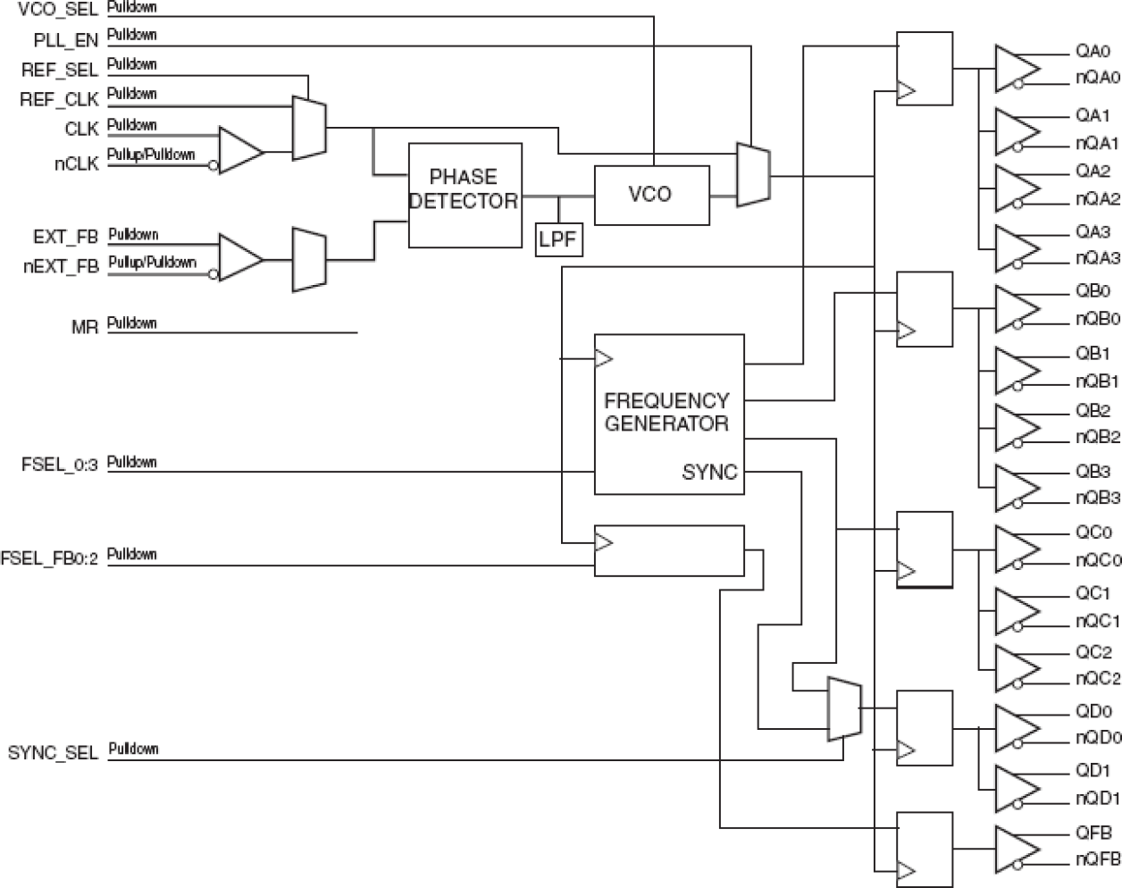
The 873991-147 is a low voltage, low skew, 3.3V LVPECL or ECL Clock Generator and a member of the family of High Performance Clock Solutions from IDT. The 873991-147 has two selectable clock inputs. The CLK, nCLK pair can accept LVPECL, LVDS, LVHSTL, SSTL and HCSL input levels and, the REF_CLK pin can accept a LVCMOS or LVTTL input levels. This device has a fully integrated PLL along with frequency configurable outputs. An external feedback input and output regenerates clocks with "zero delay". The four independent banks of outputs each have their own output dividers, which allow the device to generate a multitude of different bank frequency ratios and output-to-input frequency ratios. The output frequency range is 25MHz to 480MHz and the input frequency range is 6.25MHz to 120MHz. The PLL_EN input can be used to bypass the PLL for test and system debug purposes. In bypass mode, the input clock is routed around the PLL and into the internal output dividers. The 873991-147 also has a SYNC output which can be used for system synchronization purposes. It monitors Bank A and Bank C outputs for coincident rising edges and signals a pulse per the timing diagrams in this data sheet. This feature is used primarily in applications where Bank A and Bank C are running at different frequencies, and is particularly useful when they are running at non-integer multiples of each other.

