封装信息
| CAD 模型: | View CAD Model |
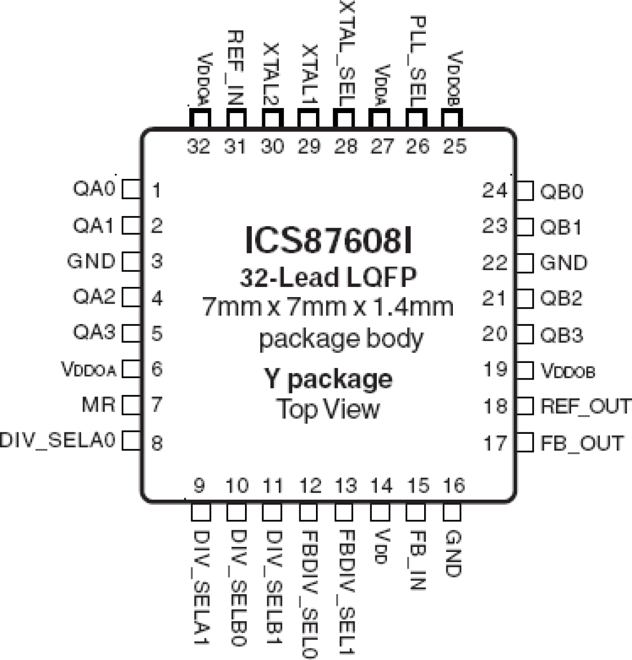
| Pkg. Type: | TQFP |
| Pkg. Code: | PRG32 |
| Lead Count (#): | 32 |
| Pkg. Dimensions (mm): | 7.0 x 7.0 x 1.4 |
| Pitch (mm): | 0.8 |
环境和出口类别
| Moisture Sensitivity Level (MSL) | 3 |
| Pb (Lead) Free | Yes |
| ECCN (US) | EAR99 |
| HTS (US) | 8542.39.0090 |
产品属性
| Lead Count (#) | 32 |
| Carrier Type | Reel |
| Moisture Sensitivity Level (MSL) | 3 |
| Qty. per Reel (#) | 2000 |
| Qty. per Carrier (#) | 0 |
| Pb (Lead) Free | Yes |
| Pb Free Category | e3 Sn |
| Temp. Range (°C) | -40 to 85°C |
| Advanced Features | Feedback Input, Reference Output |
| App Jitter Compliance | PCI/PCI-X |
| C-C Jitter Max P-P (ps) | 120 |
| Core Voltage (V) | 3.3 |
| Feedback Input | Yes |
| Input Freq (MHz) | 8.33 - 41.67 |
| Input Type | Crystal, LVCMOS |
| Inputs (#) | 2 |
| Length (mm) | 7 |
| MOQ | 2000 |
| Output Banks (#) | 3 |
| Output Freq Range (MHz) | 8.33 - 166.67 |
| Output Skew (ps) | 250 |
| Output Type | LVCMOS, LVTTL |
| Output Voltage (V) | 2.5V, 3.3V |
| Outputs (#) | 10 |
| Package Area (mm²) | 49 |
| Period Jitter Max P-P (ps) | 20 |
| Pitch (mm) | 0.8 |
| Pkg. Dimensions (mm) | 7.0 x 7.0 x 1.4 |
| Pkg. Type | TQFP |
| Prog. Clock | No |
| Reel Size (in) | 13 |
| Reference Output | Yes |
| Requires Terms and Conditions | Does not require acceptance of Terms and Conditions |
| Spread Spectrum | No |
| Tape & Reel | Yes |
| Thickness (mm) | 1.4 |
| Width (mm) | 7 |
| 已发布 | No |
有关 87608I 的资源
描述
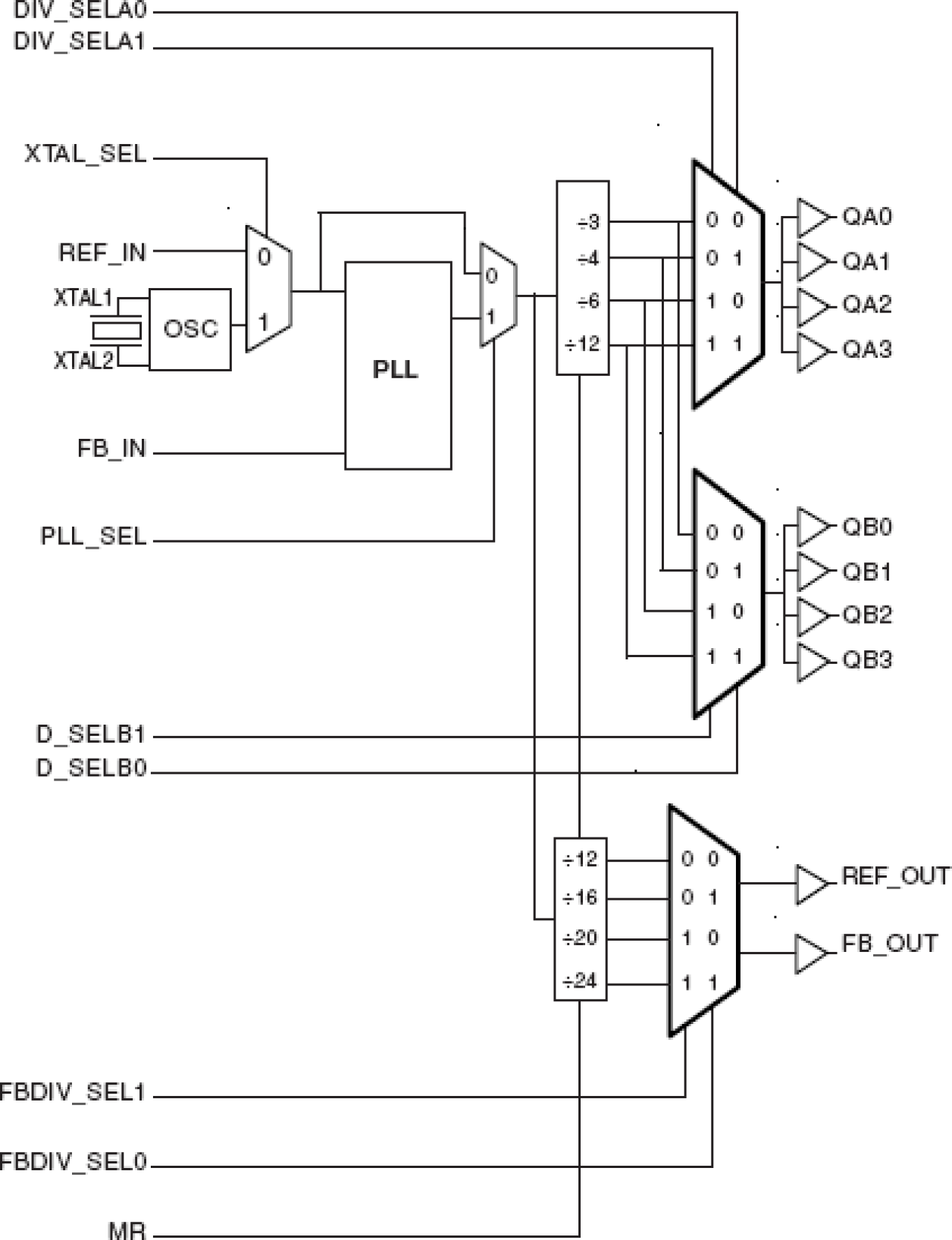
The 87608I has a selectable REF_CLK or crystal input. The REF_CLK input accepts LVCMOS or LVTTL input levels. The 87608I has a fully integrated PLL along with frequency configurable clock and feedback outputs for multiplying and regenerating clocks with "zero delay". The 87608I is a 1:8 PCI/PCI-X Clock Generator. The 87608I has a selectable REF_CLK or crystal input. The REF_CLK input accepts LVCMOS or LVTTL input levels. The 87608I has a fully integrated PLL along with frequency configurable clock and feedback outputs for multiplying and regenerating clocks with "zero delay". The PLL's VCO has an operating range of 250MHz-500MHz, allowing this device to be used in a variety of general purpose clocking applications. For PCI/PCI-X applications in particular, the VCO frequency should be set to 400MHz. This can be accomplished by supplying 33.33MHz, 25MHz, 20MHz, or 16.66MHz on the reference clock or crystal input and by selecting ÷12, ÷16, ÷20, or ÷24, respectively as the feedback divide value. The dividers on each of the two output banks can then be independently configured to generate 33.33MHz (÷12), 66.66MHz (÷6), 100MHz (÷4), or 133.33MHz (÷3). The 87608I is characterized to operate with its core supply at 3.3V and each bank supply at 3.3V or 2.5V. The 87608I is packaged in a small 7x7mm body LQFP, making it ideal for use in space-constrained applications.


