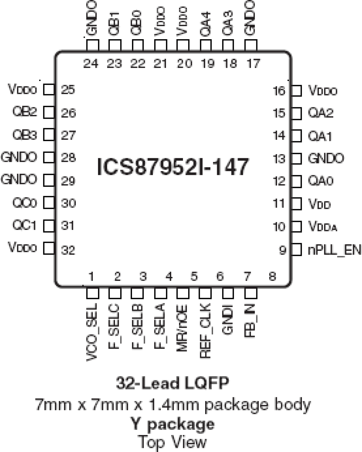
封装信息
| Pkg. Type: | TQFP |
| Pkg. Code: | PRG32 |
| Lead Count (#): | 32 |
| Pkg. Dimensions (mm): | 7.0 x 7.0 x 1.4 |
| Pitch (mm): | 0.8 |
环境和出口类别
| Moisture Sensitivity Level (MSL) | 3 |
| Pb (Lead) Free | Yes |
| ECCN (US) | EAR99 |
| HTS (US) | 8542.39.0090 |
产品属性
| Lead Count (#) | 32 |
| Carrier Type | Tray |
| Moisture Sensitivity Level (MSL) | 3 |
| Qty. per Reel (#) | 0 |
| Qty. per Carrier (#) | 250 |
| Pb (Lead) Free | Yes |
| Pb Free Category | e3 Sn |
| Temp. Range (°C) | -40 to 85°C |
| Advanced Features | Feedback Input |
| C-C Jitter Max P-P (ps) | 250 |
| Core Voltage (V) | 3.3 |
| Feedback Input | Yes |
| Input Freq (MHz) | 100 |
| Input Type | LVCMOS |
| Inputs (#) | 1 |
| Length (mm) | 7 |
| MOQ | 250 |
| Output Banks (#) | 3 |
| Output Freq Range (MHz) | 180 |
| Output Skew (ps) | 50 |
| Output Type | LVCMOS |
| Output Voltage (V) | 3.3 |
| Outputs (#) | 11 |
| Package Area (mm²) | 49 |
| Period Jitter Max P-P (ps) | 100 |
| Pitch (mm) | 0.8 |
| Pkg. Dimensions (mm) | 7.0 x 7.0 x 1.4 |
| Pkg. Type | TQFP |
| Price (USD) | $6 |
| Prog. Clock | No |
| Requires Terms and Conditions | Does not require acceptance of Terms and Conditions |
| Tape & Reel | No |
| Thickness (mm) | 1.4 |
| Width (mm) | 7 |
| 已发布 | No |
有关 87952I-147 的资源
描述
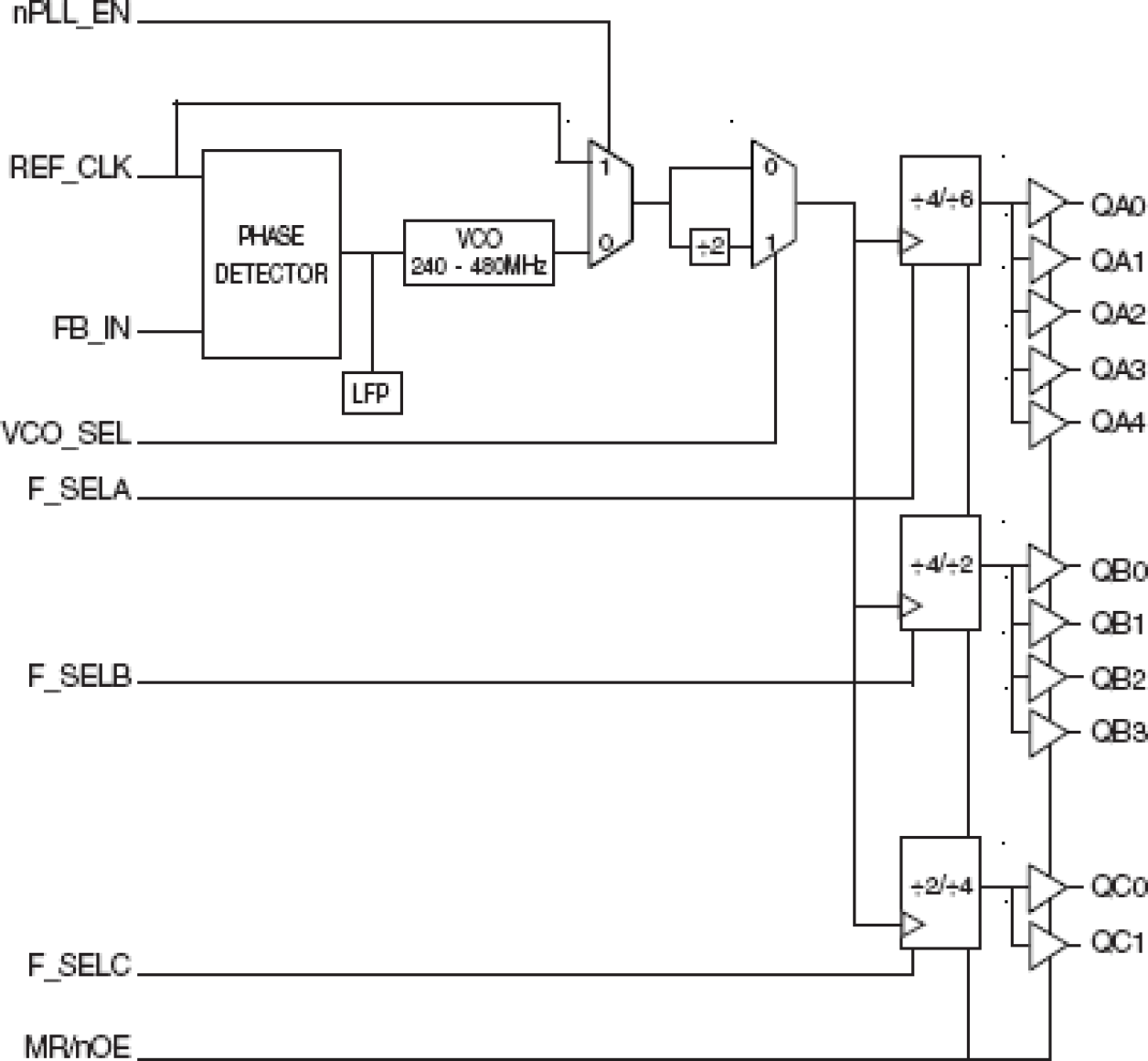
The 87952I-147 is a low voltage, low skew LVCMOS/LVTTL Clock Generator and a member of the family of High Performance Clock Solutions from IDT. With output frequencies up to 180MHz, the 87952I-147 is targeted for high performance clock applications. Along with a fully integrated PLL, the 87952I-147 contains frequency configurable outputs and an external feedback input for regenerating clocks with "zero delay". For test and system debug purposes, the nPLL_EN input allows the PLL to be bypassed. When HIGH, the MR/nOE input resets the internal dividers and forces the outputs to the high impedance state. The low impedance LVCMOS/LVTTL outputs of the 87952I- 147 are designed to drive terminated transmission lines. The effective fanout of each output can be doubled by utilizing the ability of each output to drive two series terminated transmission lines.


