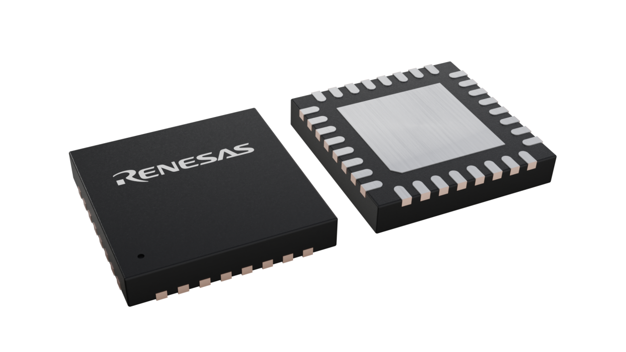
封装信息
| CAD 模型: | View CAD Model |
| Pkg. Type: | VFQFPN |
| Pkg. Code: | NLG32 |
| Lead Count (#): | 32 |
| Pkg. Dimensions (mm): | 5.0 x 5.0 x 0.9 |
| Pitch (mm): | 0.5 |
环境和出口类别
| Moisture Sensitivity Level (MSL) | 3 |
| Pb (Lead) Free | Yes |
| ECCN (US) | EAR99 |
| HTS (US) | 8542.39.0090 |
产品属性
| Lead Count (#) | 32 |
| Carrier Type | Tray |
| Moisture Sensitivity Level (MSL) | 3 |
| Qty. per Reel (#) | 0 |
| Qty. per Carrier (#) | 490 |
| Pb (Lead) Free | Yes |
| Pb Free Category | e3 Sn |
| Temp. Range (°C) | -40 to 85°C |
| Accepts Spread Spec Input | No |
| Core Voltage (V) | 2.5 |
| Feedback Input | No |
| Function | Buffer |
| Input Freq (MHz) | 800 |
| Input Type | LVPECL, LVDS, CML |
| Inputs (#) | 1 |
| Length (mm) | 5 |
| MOQ | 490 |
| Output Banks (#) | 1 |
| Output Freq Range (MHz) | 800 |
| Output Signaling | LVDS |
| Output Type | LVDS |
| Output Voltage (V) | 2.5 |
| Outputs (#) | 1 |
| Package Area (mm²) | 25 |
| Pitch (mm) | 0.5 |
| Pkg. Dimensions (mm) | 5.0 x 5.0 x 0.9 |
| Pkg. Type | VFQFPN |
| Price (USD) | $11.23982 |
| Product Category | Clock Buffers & Drivers |
| Prog. Clock | No |
| Requires Terms and Conditions | Does not require acceptance of Terms and Conditions |
| Tape & Reel | No |
| Thickness (mm) | 0.9 |
| Width (mm) | 5 |
| 已发布 | No |
有关 8S89296 的资源
描述
The 8S89296 is a high-performance LVDS programmable delay line. The delay can vary from 2.2ns to 12.5ns in 10ps steps. The 8S89296 is characterized to operate from a 2.5V power supply and is guaranteed over the industrial temperature range. The delay of the device varies in discrete steps based on a control word; a 10-bit long control word sets the delay in 10ps increments. Also, the input pins IN and nIN default to an equivalent low state when left floating. The control register can accept CMOS or TTL-level signals.
