封装信息
| Pkg. Type: | PTQFP |
| Pkg. Code: | DXG32 |
| Lead Count (#): | 32 |
| Pkg. Dimensions (mm): | 7.0 x 7.0 x 1.0 |
| Pitch (mm): | 0.8 |
环境和出口类别
| Moisture Sensitivity Level (MSL) | 3 |
| Pb (Lead) Free | Yes |
| ECCN (US) | EAR99 |
| HTS (US) | 8542.39.0090 |
产品属性
| Lead Count (#) | 32 |
| Carrier Type | Reel |
| Moisture Sensitivity Level (MSL) | 3 |
| Qty. per Reel (#) | 1000 |
| Pkg. Dimensions (mm) | 7.0 x 7.0 x 1.0 |
| Qty. per Carrier (#) | 0 |
| Package Area (mm²) | 49 |
| Pitch (mm) | 0.8 |
| Pb (Lead) Free | Yes |
| Pb Free Category | e3 Sn |
| Temp. Range (°C) | -40 to 85°C |
| Additive Phase Jitter Typ RMS (fs) | 100 |
| Additive Phase Jitter Typ RMS (ps) | 0.1 |
| Core Voltage (V) | 2.5V, 3.3V |
| Function | Buffer |
| Input Freq (MHz) | 3000 |
| Input Type | LVPECL, HSTL |
| Inputs (#) | 2 |
| Length (mm) | 7 |
| MOQ | 1000 |
| Output Banks (#) | 1 |
| Output Freq Range (MHz) | 3000 |
| Output Skew (ps) | 50 |
| Output Type | LVPECL |
| Output Voltage (V) | 2.5V, 3.3V |
| Outputs (#) | 10 |
| Pkg. Type | PTQFP |
| Product Category | Clock Buffers & Drivers |
| Reel Size (in) | 13 |
| Requires Terms and Conditions | Does not require acceptance of Terms and Conditions |
| Tape & Reel | Yes |
| Thickness (mm) | 1 |
| Width (mm) | 7 |
| 已发布 | No |
有关 8T33FS6111 的资源
描述
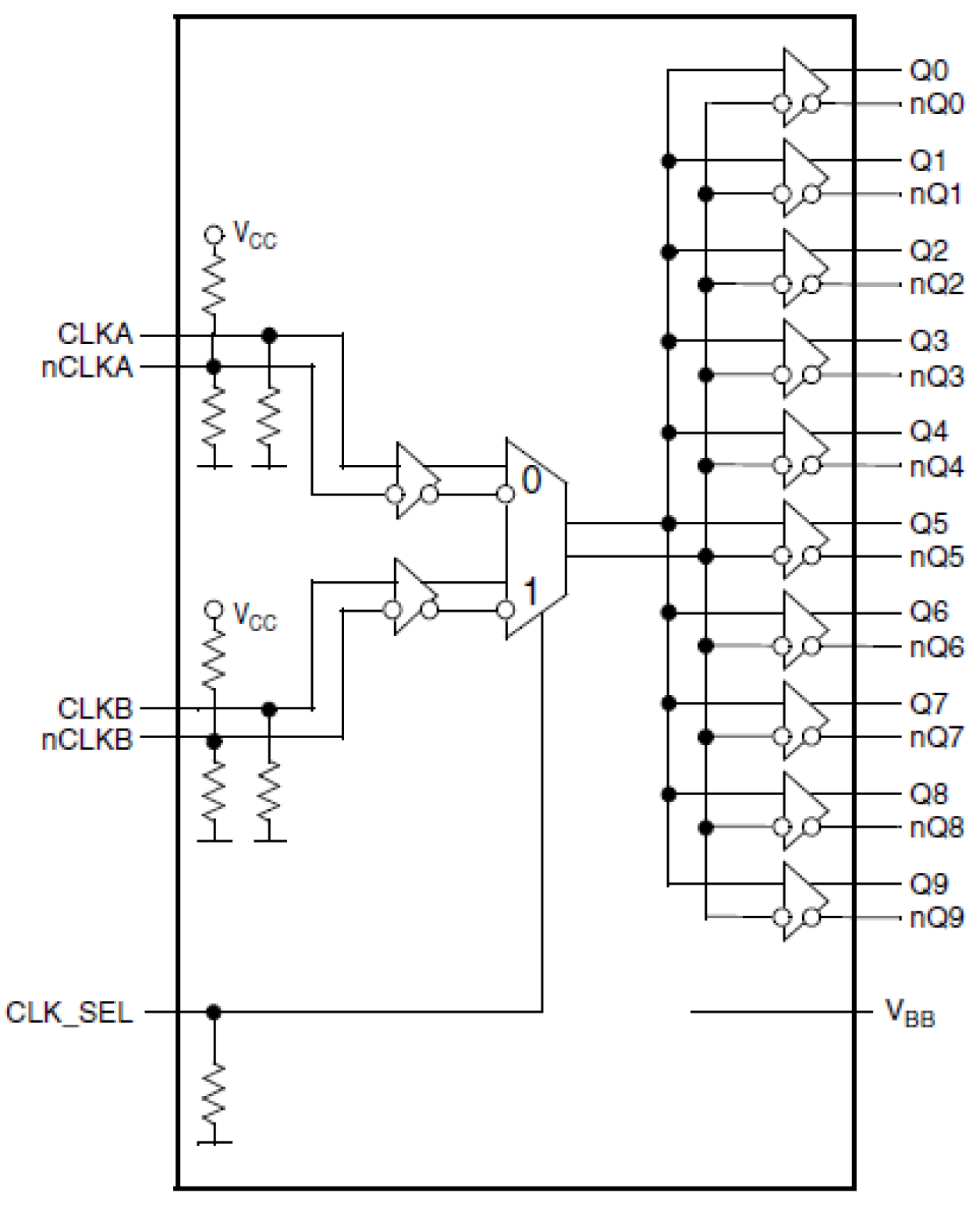
The 8T33FS6111 is a bipolar monolithic differential clock fanout buffer. Designed for the most demanding clock distribution systems, the 8T33FS6111 supports various applications that require the distribution of precisely aligned differential clock signals. Using SiGe:C technology and a fully differential architecture, the device offers very low skew outputs and superior digital signal characteristics. The target application for this clock driver is high-performance clock distribution in computing, networking, and telecommunication systems.
The 8T33FS6111 is designed for low-skew clock distribution systems and supports clock frequencies up to 2.7GHz. The device accepts two clock sources. The CLKA input can be driven by LVPECL compatible signals, the CLKB input accepts HSTL or LVPECL compatible signals. The selected input signal is distributed to 10 identical, LVPECL outputs. If VBB is connected to the CLKA input and bypassed to GND by a 10nF capacitor, the 8T33FS6111 can be driven by single-ended LVPECL signals utilizing the VBB bias voltage output.
To meet the tight skew specification of the device, both outputs of a differential output pair should be terminated, even if only one output is used. In the case where not all ten outputs are used, the output pairs on the same package side as the parts being used on that side should be terminated. The 8T33FS6111 can be operated from a single 3.3V or 2.5V supply.

