封装信息
| CAD 模型: | View CAD Model |
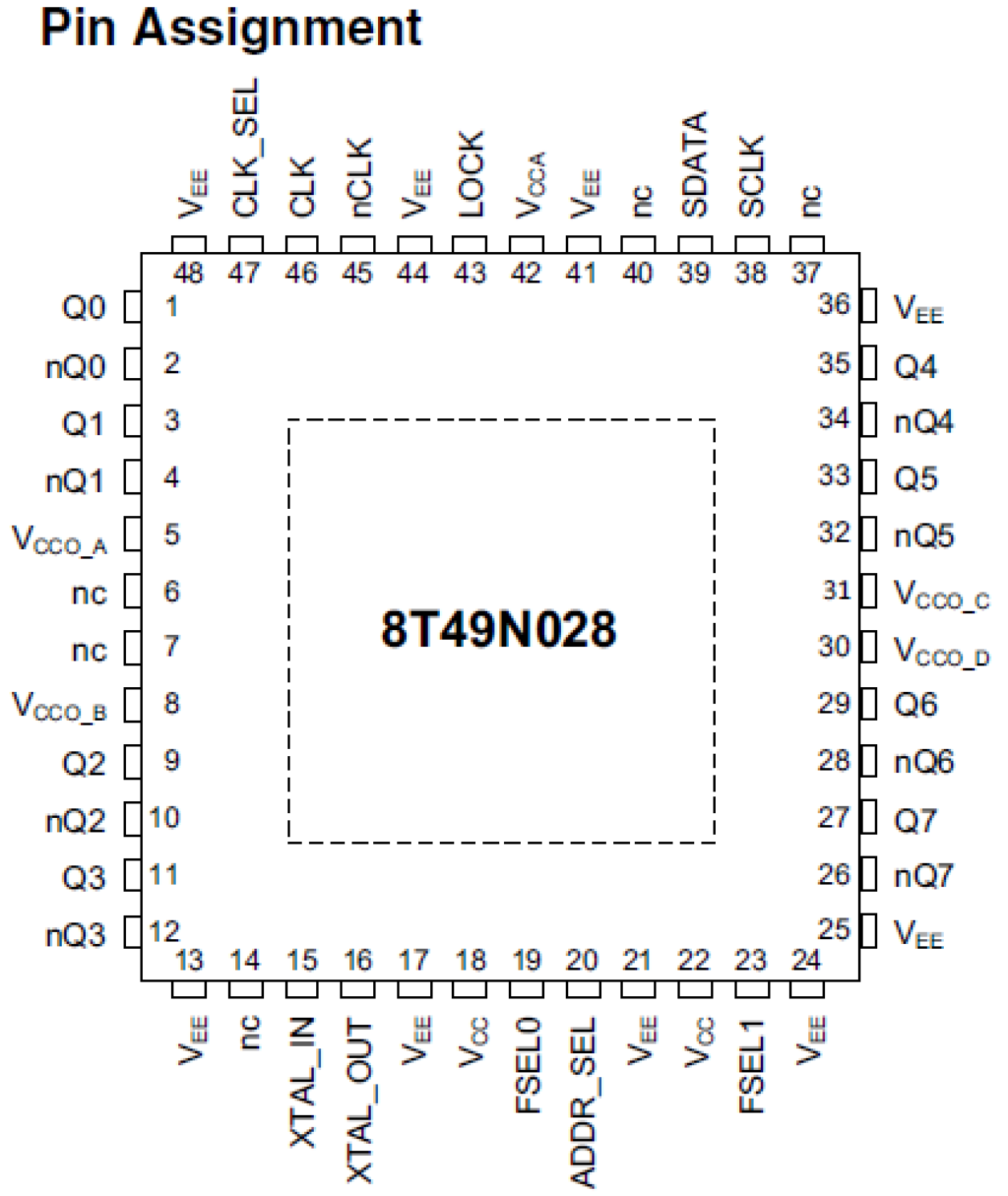
| Pkg. Type: | VFQFPN |
| Pkg. Code: | NLG48 |
| Lead Count (#): | 48 |
| Pkg. Dimensions (mm): | 7.0 x 7.0 x 0.9 |
| Pitch (mm): | 0.5 |
环境和出口类别
| Moisture Sensitivity Level (MSL) | 3 |
| Pb (Lead) Free | Yes |
| ECCN (US) | EAR99 |
| HTS (US) | 8542.39.0090 |
产品属性
| Lead Count (#) | 48 |
| Carrier Type | Reel |
| Moisture Sensitivity Level (MSL) | 3 |
| Qty. per Reel (#) | 2000 |
| Qty. per Carrier (#) | 0 |
| Pb (Lead) Free | Yes |
| Pb Free Category | e3 Sn |
| Temp. Range (°C) | -40 to 85°C |
| Advanced Features | Programmable Clock |
| Core Voltage (V) | 3.3V, 2.5V |
| Divider Value | 2 |
| Family Name | FemtoClock NG |
| Feedback Divider | 16 - 250 |
| Feedback Input | No |
| Input Freq (MHz) | 10 - 312.5 |
| Input Type | Crystal, LVPECL, LVDS, HCSL |
| Inputs (#) | 2 |
| Length (mm) | 7 |
| MOQ | 2000 |
| Output Banks (#) | 4 |
| Output Freq Range (MHz) | 15.16 - 1250 |
| Output Signaling | LVPECL, LVDS |
| Output Skew (ps) | 50 |
| Output Type | LVPECL, LVDS |
| Output Voltage (V) | 3.3V, 2.5V |
| Outputs (#) | 8 |
| Package Area (mm²) | 49 |
| Period Jitter Max P-P (ps) | 8.3 |
| Period Jitter Typ P-P (ps) | 0.78 |
| Phase Jitter Max RMS (ps) | 0.292 |
| Phase Jitter Typ RMS (fs) | 212 |
| Phase Jitter Typ RMS (ps) | 0.212 |
| Pitch (mm) | 0.5 |
| Pkg. Dimensions (mm) | 7.0 x 7.0 x 0.9 |
| Pkg. Type | VFQFPN |
| Prog. Clock | Yes |
| Prog. Interface | I2C |
| Reel Size (in) | 13 |
| Reference Output | Yes |
| Requires Terms and Conditions | Does not require acceptance of Terms and Conditions |
| Spread Spectrum | No |
| Tape & Reel | Yes |
| Thickness (mm) | 0.9 |
| VCO Max Freq (MHz) | 2500 |
| VCO Min Freq (MHz) | 1910 |
| Width (mm) | 7 |
| Xtal Freq (KHz) | 10 - 40 |
| Xtal Inputs (#) | 1 |
| 已发布 | No |
有关 8T49N028 的资源
描述
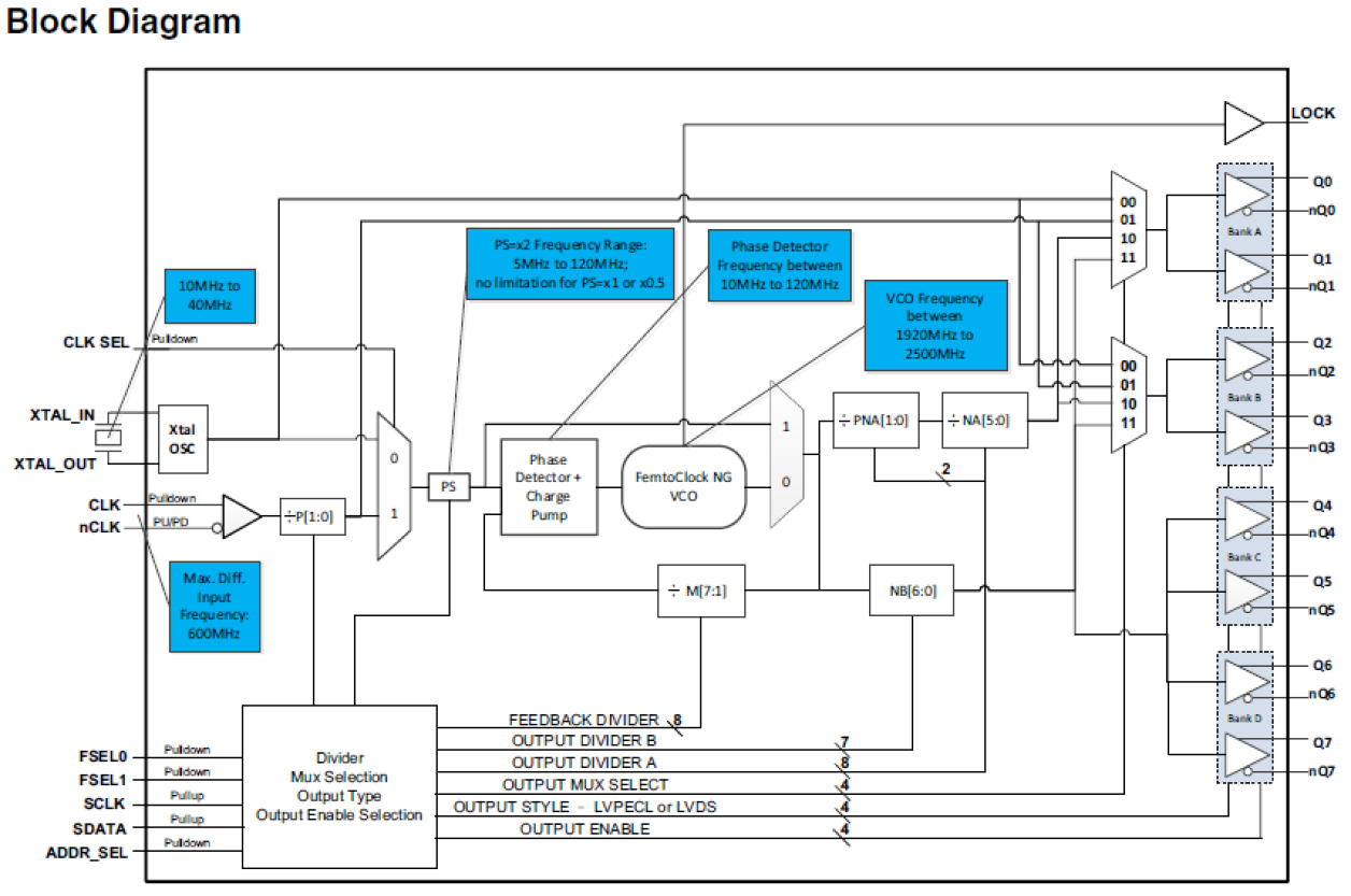
The 8T49N028 is a low RMS phase jitter clock synthesizer with selectable internal crystal oscillator or external clock references and eight outputs, configurable as either LVDS, LVPECL, or high impedance.
After power up, two frequency select pins determine one of up to four different sets of factory preprogrammed crystal or input frequency and output frequency configurations. From a single input reference, as many as three different output frequencies may be selected for the output banks: two of these frequencies can be generated by the internal crystal oscillator, and/or external clock pre-divider, and/or A output divider, and/or B output divider. The third output frequency is from the B output divider. Device pre-programming can be overwritten through the provided I2C interface.
The specific internal register settings for each of the four frequency sets are specified by a Renesas order code. Custom codes can be provided by contacting Renesas.

