封装信息
| CAD 模型: | View CAD Model |
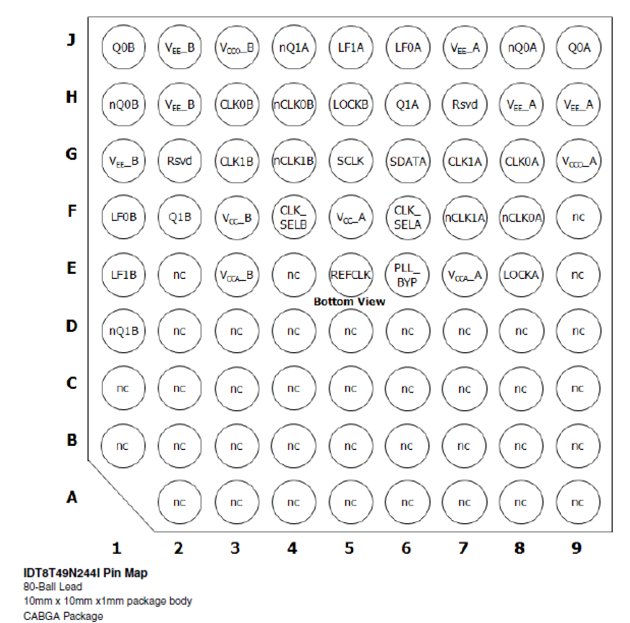
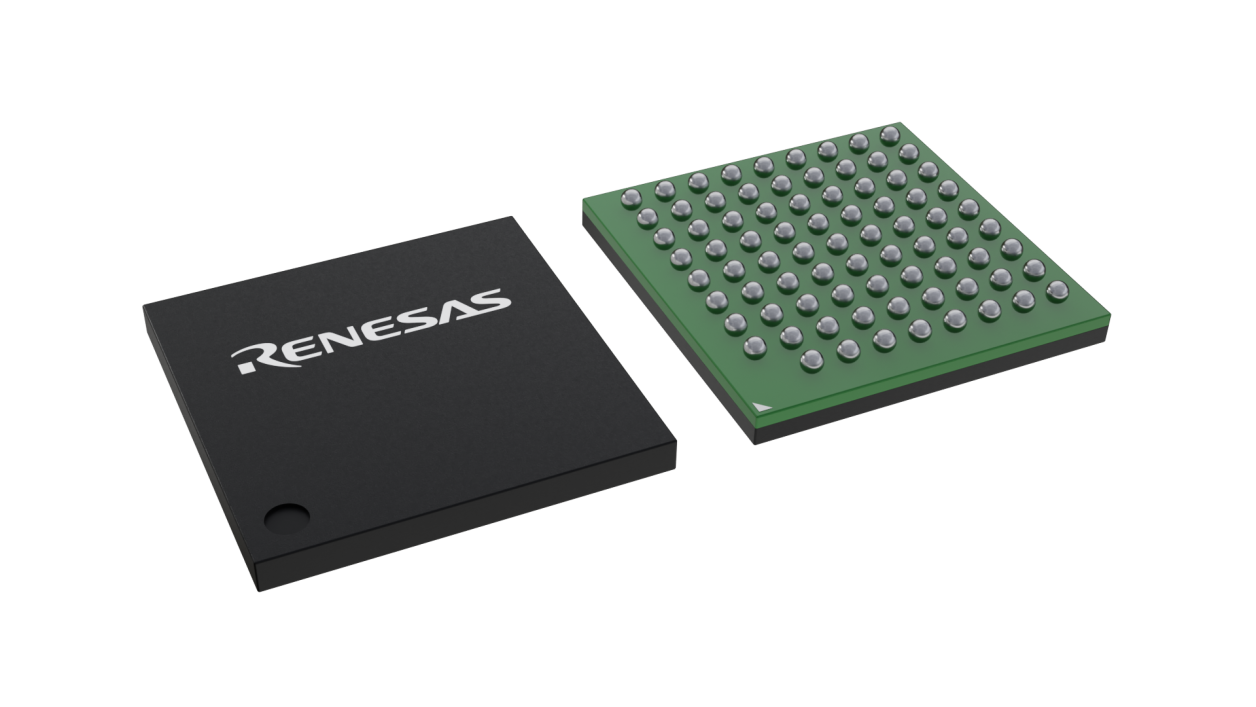
| Pkg. Type: | CABGA |
| Pkg. Code: | ASG80 |
| Lead Count (#): | 80 |
| Pkg. Dimensions (mm): | 10.0 x 10.0 x 1.4 |
| Pitch (mm): | 1 |
环境和出口类别
| Pb (Lead) Free | Yes |
| ECCN (US) | EAR99 |
| HTS (US) | 8542.39.0090 |
| Moisture Sensitivity Level (MSL) | 3 |
产品属性
| Pkg. Type | CABGA |
| Lead Count (#) | 80 |
| Pb (Lead) Free | Yes |
| Carrier Type | Tray |
| Advanced Features | Programmable Clock |
| C-C Jitter Max P-P (ps) | 40 |
| Core Voltage (V) | 2.5V, 3.3V |
| Family Name | UFT |
| Feedback Input | No |
| Input Freq (MHz) | 0.008 - 710 |
| Input Type | LVCMOS, LVTTL, HCSL, LVHSTL, LVDS, LVPECL |
| Inputs (#) | 5 |
| Length (mm) | 10 |
| MOQ | 184 |
| Moisture Sensitivity Level (MSL) | 3 |
| Output Banks (#) | 2 |
| Output Freq Range (MHz) | 0.98 - 1300 |
| Output Signaling | LVPECL, LVDS |
| Output Type | LVPECL, LVDS |
| Output Voltage (V) | 2.5 |
| Outputs (#) | 4 |
| Package Area (mm²) | 100 |
| Pb Free Category | e1 SnAgCu |
| Phase Jitter Max RMS (ps) | 0.486 |
| Phase Jitter Typ RMS (fs) | 323 |
| Phase Jitter Typ RMS (ps) | 0.323 |
| Pitch (mm) | 1 |
| Pkg. Dimensions (mm) | 10.0 x 10.0 x 1.4 |
| Prog. Clock | Yes |
| Prog. Interface | I2C |
| Qty. per Carrier (#) | 184 |
| Qty. per Reel (#) | 0 |
| Reference Output | No |
| Requires Terms and Conditions | Does not require acceptance of Terms and Conditions |
| Spread Spectrum | Yes |
| Tape & Reel | No |
| Temp. Range (°C) | -40 to 85°C |
| Thickness (mm) | 1.4 |
| VCO Max Freq (MHz) | 2600 |
| VCO Min Freq (MHz) | 1995 |
| Width (mm) | 10 |
有关 8T49N244I 的资源
描述
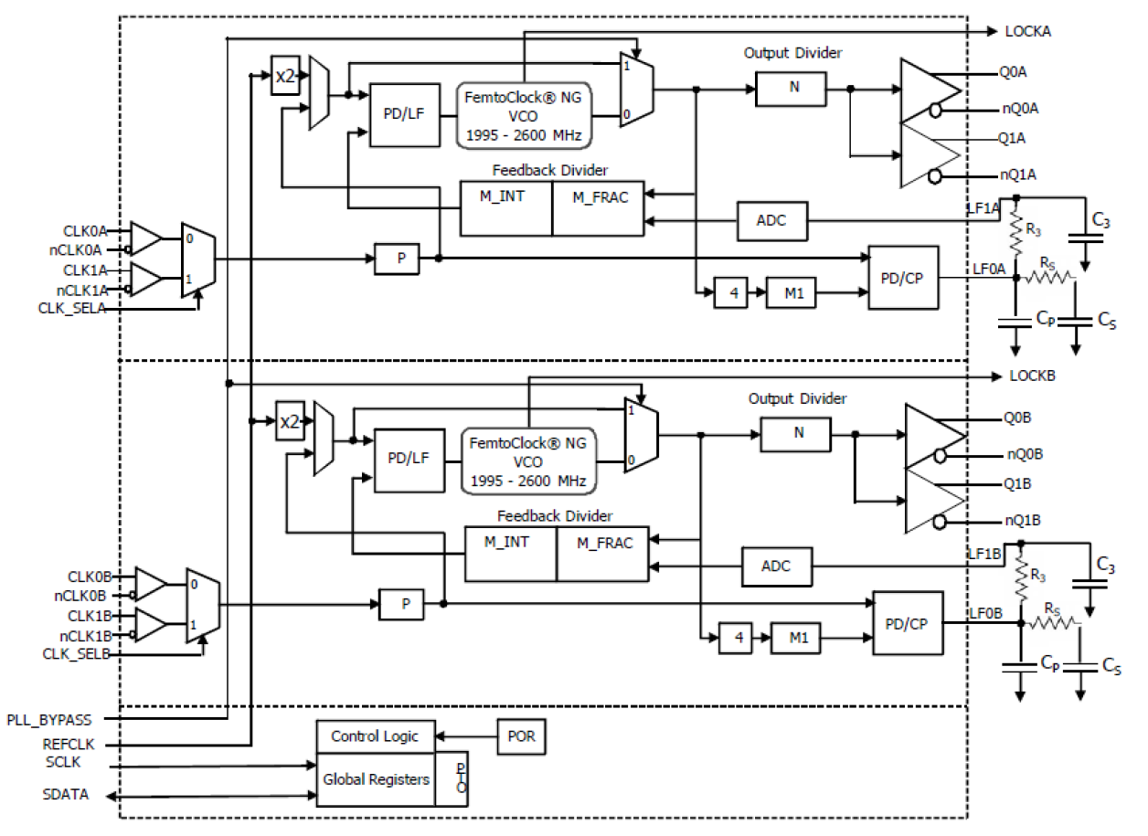
The 8T49N244I is a dual PLL using FemtoClock® NG technology. It integrates low phase noise frequency translation/synthesis and jitter attenuation. The device includes alarm and monitoring functions suitable for networking and communications applications. It has two fully independent PLLs. Each PLL can generate any output frequency in the 0.98MHz to 312.5MHz range and most output frequencies in the 312.5MHz to 1,300MHz range. A wide range of input reference clocks may be used as the source for the output frequencies.
Each PLL has three operating modes to support a very broad spectrum of applications: Frequency Synthesizer, High-Bandwidth Frequency Translator, and Low-Bandwidth Frequency Translator.


