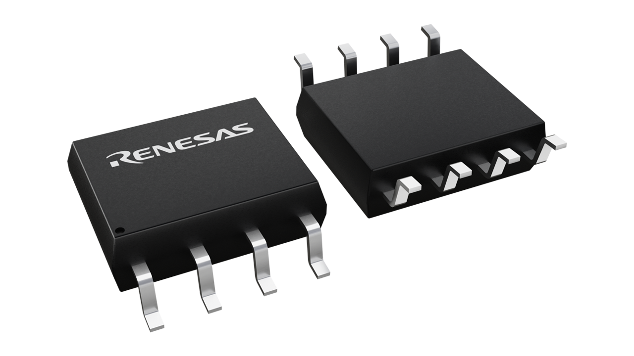

封装信息
| CAD 模型: | View CAD Model |
| Pkg. Type: | SOIC |
| Pkg. Code: | DCG8 |
| Lead Count (#): | 8 |
| Pkg. Dimensions (mm): | 4.9 x 3.9 x 1.5 |
| Pitch (mm): | 1.27 |
环境和出口类别
| Pb (Lead) Free | Yes |
| ECCN (US) | EAR99 |
| HTS (US) | 8542.39.0090 |
| Moisture Sensitivity Level (MSL) | 1 |
产品属性
| Pkg. Type | SOIC |
| Lead Count (#) | 8 |
| Pb (Lead) Free | Yes |
| Carrier Type | Tube |
| Accepts Spread Spec Input | Yes |
| Advanced Features | Accepts Spread Spec Input |
| C-C Jitter Max P-P (ps) | 300 |
| C-C Jitter Typ P-P (ps) | 125 |
| Core Voltage (V) | 5 |
| Feedback Input | Yes |
| Input Freq (MHz) | 8 - 80 |
| Input Type | LVCMOS |
| Inputs (#) | 4 |
| Length (mm) | 4.9 |
| MOQ | 97 |
| Moisture Sensitivity Level (MSL) | 1 |
| Output Banks (#) | 2 |
| Output Freq Range (MHz) | 20 - 80 |
| Output Type | LVCMOS |
| Output Voltage (V) | 5 |
| Outputs (#) | 2 |
| Package Area (mm²) | 19.1 |
| Pb Free Category | e3 Sn |
| Period Jitter Max P-P (ps) | 500 |
| Pitch (mm) | 1.27 |
| Pkg. Dimensions (mm) | 4.9 x 3.9 x 1.5 |
| Price (USD) | $5.26 |
| Prog. Clock | No |
| Qty. per Carrier (#) | 97 |
| Qty. per Reel (#) | 0 |
| Requires Terms and Conditions | Does not require acceptance of Terms and Conditions |
| Supply Voltage (V) | 5 - 5 |
| Tape & Reel | No |
| Temp. Range (°C) | 0 to 70°C |
| Thickness (mm) | 1.5 |
| Width (mm) | 3.9 |
有关 9170B-01 的资源
描述
The IDT9170B generates an output clock which is synchronized to a given continuous input clock with zero delay (±1ns at 5 V VDD). Using IDT's proprietary phase-locked loop (PLL) analog CMOS technology, the IDT9170B is useful for regenerating clocks in high speed systems where skew is a major concern. By the use of the two select pins, multiples or divisions of the input clock can be generated with zero delay (see Tables 2 and 3). The standard versions produce two outputs, where CLK2 is always a divide by two version of CLK1. The IDT9170B is also useful to recover poor duty cycle clocks. A 50 MHz signal with a 20/80% duty cycle, for example, can be regenerated to the 48/52% typical of the part. The IDT9170B allows the user to control the PLL feedback, making it possible, with an additional 74F240 octal buffer (or other such device that offers controlled skew outputs), to synchronize up to 8 output clocks with zero delay compared to the input. Application notes for the IDT9170B are available. Please consult IDT.