特性
- Six 0.7V current mode differential HCSL output pairs
- One differential clock input
- CLK and nCLK supports the following input types: LVPECL, LVDS, LVHSTL, SSTL, HCSL
- Maximum output frequency: 140MHz
- Input frequency range: 90MHz - 140MHz
- VCO range: 450MHz - 700MHz
- Output skew: 110ps (maximum)
- Cycle-to-Cycle jitter: 110ps (maximum)
- RMS phase jitter @ 100MHz, (1.5MHz - 22MHz): 2.42ps (typical)
- 3.3V operating supply
- 0°C to 70°C ambient operating temperature
- Available in lead-free RoHS compliant package
- Industrial temperature information available upon request
描述
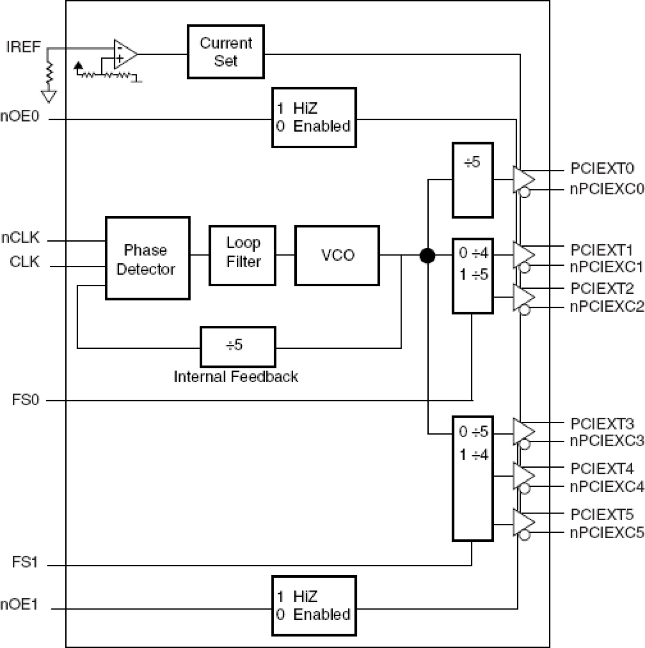
The 9DB206 is a high performance 1-to-6 Differential-to-HCSL Jitter Attenuator designed for use in PCI Express®™ systems. In some PCI Express® systems, such as those found in desktop PCs, the PCI Express® clocks are generated from a low bandwidth, high phase noise PLL frequency synthesizer. In these systems, a jitter-attenuating device may be necessary in order to reduce high frequency random and deterministic jitter components from the PLL synthesizer and from the system board. The 9DB206 has two PLL bandwidth modes. In low bandwidth mode, the PLL loop bandwidth is 500kHz. This setting offers the best jitter attenuation and is still high enough to pass a triangular input spread spectrum profile. In high bandwidth mode, the PLL bandwidth is at 1MHz and allows the PLL to pass more spread spectrum modulation. For serdes which have x10 reference multipliers instead of x12.5 multipliers, 5 of the 6 PCI Express® outputs (PCIEX1:5) can be set for 125MHz instead of 100MHz by configuring the appropriate frequency select pins (FS0:1). Output PCIEX0 will always run at the reference clock frequency (usually 100MHz) in desktop PC PCI Express® Applications.
当前筛选条件


