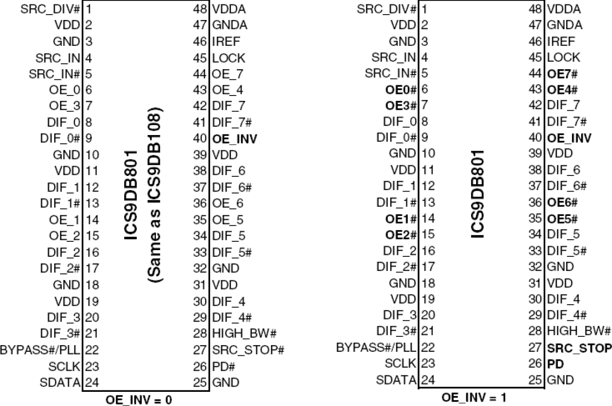
特性
- 8 - 0.7 V current-mode differential output pairs
- Supports zero delay buffer mode and fanout mode
- Bandwidth programming available
- Spread spectrum modulation tolerant, 0 to -0.5% down spread and +/- 0.25% center spread.
- Supports undriven differential outputs in PD# and SRC_STOP# modes for power management.
- Supports polarity inversion to the output enables, SRC_STOP and PD.
- Outputs cycle-cycle jitter < 50 ps
- Outputs skew: 50 ps
- 50 - 200 MHz operation
- Extended frequency range in bypass mode to 400 MHz
- PCI Express® Gen I compliant
- Real time PLL lock detect output pin
- 48-pin SSOP/TSSOP package
- Available in RoHS compliant packaging
描述
The 9DB801C is a DB800 Version 2.0 Yellow Cover part with PCI Express® support. It can be used in PC or embedded systems to provide outputs that have low cycle-to-cycle jitter (50 ps), low output-to-output skew (100 ps), and are PCI Express® gen 1 compliant. The 9DB801C supports a 1 to 8 output configuration, taking a spread or non spread differential HCSL input from a CK410(B) main clock such as 954101 and 932S401, or any other differential HCSL pair. 9DB801C can generate HCSL or LVDS outputs from 50 to 200 MHz in PLL mode or 0 to 400 MHz in bypass mode. There are two de-jittering modes available selectable through the HIGH_BW# input pin, high bandwidth mode provides de-jittering for spread inputs and low bandwidth mode provides extra de-jittering for non-spread inputs. The SRC_STOP#, PD#, and individual OE# real-time input pins provide completely programmable power management control.
当前筛选条件
筛选
软件与工具
样例程序
模拟模型
This is the first video in our PCIe series. In this video, we define PCIe architectures, focusing on common and separate clock architectures. Watch the rest of the video series below where Ron will cover the impact of different timing architectures.
Watch the Video Series Below
In this episode, Ron Wade from IDT (acquired by Renesas) explains PCIe common clocking and its impact on timing solutions. Learn about using a single clock source, fan-out buffers, and the considerations for spread spectrum and non-spread spectrum clocking in PCIe systems.
Watch the Video Series Below
- PCIe Clocking Architectures (Common and Separate)
- PCIe Separate Reference without Spread Clock Architecture
- PCIe Separate Reference Clock With Independent Spread (SRIS) Architecture Overview
Transcript
Hi, this is Ron Wade again with IDT. Today in this little episode we're gonna talk about PCI Express common clocking and its impact on the timing solutions that you would use in the system. So, as the name implies, common clocking says that all of the clocks come from one source. In this case it's a PLL. It may be spreading, it may not, but very seldom do you get all of your clocks from one device, so you'll need some sort of fan out buffers to distribute extra copies of the PCI Express clocks.
And while it's still a common clock, now we have to take into account whether we're using spread spectrum or whether we're using non-spread spectrum. If we are not using SFC, then we can fan out to these buffers here, and this could be a ZDB with a PLL inside, or it could be a fan out buffer, or it could be a part where you select between the two. Without spread spectrum, I can put this buffer in PLL mode or ZDB mode, it doesn't really matter and I don't violate the common clock requirement from the PCI Express sig. Same with this guy, it could be a fan out buffer or a PLL, ZDB, it doesn't really matter.
Things get really interesting though when spread spectrum is in use. When spread spectrum is in use then I have to have...this is my common clock. With spread spectrum in use, these have to be in fan out buffer mode. They cannot be used in PLL mode. And there's a couple of reasons for that, the simplest reason is that if this were a PLL, ZDB and it is tracking the spread, there will always be some tracking error, which means that as the input clock goes like this, the output clock is gonna overshoot it and go down like that. That's just the nature of having a PLL with finite bandwidth. So, you have tracking error here, and the tracking error will cause this to fall out of the PCI Express PPM limitations of +5,300 to -5,300 when you're using a half percent down-spread clock. So with SFC, you have your spread spectrum clock generator but any fan out buffer, any buffering at all has to be a fan out buffer without a PLL. That's a limitation on the architecture.
So the other point I'd like to make is as far as the jitter is concerned, because we're using a common clock here, to assume that the jitter on both sides for the clock is the same and all we have to do is take the difference function...that's a minus sign...the difference between the CPU and the CPU transmitter, say in the I/O storage receiver to calculate our jitter. That'll be more important when we get to the separate clocking in a future video.
In this video, we explore PCIe with separate reference clocks and the effects of clock selection. Learn how separate reference clocks work and their impact on system performance and stability.
Watch the Video Series Below
- Edit Video page PCIe Clocking Architectures (Common and Separate)
- PCIe Common Clock Architecture and its Impact on Clocking
- PCIe Separate Reference Clock With Independent Spread (SRIS) Architecture Overview
This video provides a high-level overview of Separate Reference Clock with Independent Spread (SRIS) architectures for PCI Express systems, additional performance requirements that this clocking architecture imposes on the reference clocks, and some system implications encountered trying to implement the architecture.
Watch the Video Series Below
- PCIe Clocking Architectures (Common and Separate)
- PCIe Common Clock Architecture and its Impact on Clocking
- PCIe Separate Reference without Spread Clock Architecture
Transcript
Hi, there. This is Ron Wade with IDT, and we're going to talk about separate reference independence spread today, which is the latest PCI express clocking architecture. So let's jump right in and define it and see what the implications are. So we have the CPU block here and we have our IO storage block here, and in this case they're both being clocked by a spreading clock source, two separate spreading clock sources, and we have the PCI link between them. So the whole idea of doing this is to keep from having to send the clock over this, let's say it's a cable, keep it from sending a clock over the cable like you have to do today.
So one of the implications of this, one is you don't have to send the clock over the cable when you have an SRIS system, but there's some other things to take into account, too. The first is the minimum PPM on this spreading clock is minus 5300 for the PCI, say. The maximum is plus 300 PPM. In this situation, this clock could be at minus 53. This could be at 300, but that means is that this link here has to...the controllers have to, number one, know they're in SRIS mode, and then insert what's called the skip ordered set or dummy data into the link. When you do that, you're going to lose from 1 to 3% of your performance. And the second issue here is there's no mechanism today for the ends of the link to know that they need to be in SRIS mode to insert those skip ordered sets. So there's no mechanism to say, "Hey, SRIS mode, please."
So the second item or the next item is that besides the difference in jitter performance between the transmitter and the receiver and the difference between the jitter of the clock over here and the clock over here, now we have two separate spreads to take into account, and I've drawn the frequency harmonics, the 32 kilohertz of harmonics here. So these have to be taken into account so there's a difference of the spreads also has to be noted. So it's much more stringent to have a clock that meets this requirement than the other architectures already discussed.
So the specifications, they're not final from the PCI-SIG on what a clock has to do to meet these requirements. Based on early indicators, we believe that we have clocks that are SRIS compatible today, and we can talk with you much more about that on one-on-one. So that's a high level overview of SRIS, a couple of system architectures you usually have to look out for, and if you have any questions, you can email me at [email protected]. Thanks.